
Related Manuals for ADLINK Technology IMB-C47H


Summary of Contents for ADLINK Technology IMB-C47H
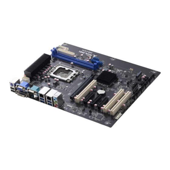
- Page 1 IMB-C47H User’s Manual ATX Motherboard with 12th/13th/14th Gen Intel ® Core™ i9/i7/i5/i3 Processors and Intel H610 Chipset ® Manual Rev.: 0.1 Preliminary Revision Date: October 08, 2024 Part Number: 50M-13020-1000...
-
Page 2: Environmental Responsibility
Preface Copyright Copyright 2024 ADLINK Technology, Inc. This document contains proprietary information protected by copyright. All rights are reserved. No part of this manual may be reproduced by any mechanical, electronic, or other means in any form without prior written permission of the manufacturer. -
Page 3: Revision History
IMB-C47 Revision History Revision Description Date Preliminary release 2024-10-08 Preface... -
Page 4: Table Of Contents
Table of Contents Preface ..........................ii List of Figures ........................vi List of Tables ........................vi Introduction ........................ 1 Packing List ........................ 1 Optional Accessories ....................1 Specifications ......................3 Core System ....................... 3 I/O Interface ........................ 4 Video ........................... 4 Audio ........................... -
Page 5: Preface
IMB-C47 Save & Exit ....................... 36 Safety Instructions ......................37 Getting Services ....................... 38 Preface... - Page 6 List of Figures Figure 1: Functional Block Diagram ......................6 Figure 2: IO Panel Connector Locations ....................7 Figure 3: Onboard Connector – Header and Jumper Locations ..............8 Figure 4: Mechanical Dimensions ......................11 Figure 5: Mechanical Dimensions - IO Panel ..................11 List of Tables Table 1: IMB-C47 Series ..........................1 Table 2: IOPanel Connector Definitions ....................7 Table 3: Onboard Connector –...
-
Page 7: Introduction
It includes high-speed data transfer interfaces such as PCIe 4.0, USB 3.0, and SATA 6 Gb/s (SATA III), and dual-channel DDR4 3200 MHz RAM for industrial automation applications. With industrial-grade I/O port design, the IMB-C47H offers a significant competitive advantage for embedded computing applications in terms of device compatibility, durable connectivity, and extreme environment readiness. - Page 8 This page intentionally left blank. Introduction...
-
Page 9: Specifications
IMB-C47 2 Specifications 2.1 Core System CPU: Family Number CPU Core Frequency (GHz) Cache(MB) Power Raptor Lake-S Refresh i9-14900T 1.1GHz 36MB Raptor Lake-S Refresh i9-14900 2.0GHz 36MB Raptor Lake-S Refresh i7-14700T 1.3GHz 33MB Raptor Lake-S Refresh i7-14700 2.1GHz 33MB Raptor Lake-S Refresh i5-14500T 1.7GHz... -
Page 10: I/O Interface
I/O Interface Expansion slots: • 1x PCIe Gen4 x16 3x PCIe x4 (Support PCIe Gen3 x2 signal, slot3 co-lay with M.2 M-key 2242/2280) • 3x PCI • SATA: 4x SATA 6.0 Gb/s connectors, SATA1 co-lay with M.2 M-key 2242/2280 ... -
Page 11: Humidity
IMB-C47 2.7 Humidity 60° C at 95% RH, non-condensing 2.8 Certificate (EMC) CE/FCC Class A 2.9 Form Factor ATX: 305 mm x 244 mm (W x L) 2.10 Operating Systems Microsoft® Windows® 10, 64-bit Microsoft® Windows® 11, 64-bit ... -
Page 12: Functional Block Diagram
2.11 Functional Block Diagram Figure 1: Functional Block Diagram Specifications... -
Page 13: Mechanical Layout
IMB-C47 3 Mechanical Layout 3.1 IO Panel Connector Locations Figure 2: IO Panel Connector Locations Table 2: IOPanel Connector Definitions Item Description Description PS/2_USB1 (PS/2) PS/2 Connector (Keyboard & Mouse) DVI_VGA1 (VGA) VGA DB15 Connector COM1 COM1 Connector RJ45_USB1 (LAN1) GBE LAN RJ45 Connector1 RJ45_USB2 (LAN2) GBE LAN RJ45 Connector2... -
Page 14: Figure 3: Onboard Connector - Header And Jumper Locations
45- 45- 25-5 25-4 25-2 25-3 25-1 Figure 3: Onboard Connector – Header and Jumper Locations Mechanical Layout... -
Page 15: Table 3: Onboard Connector - Header And Jumper Definitions
IMB-C47 Table 3: Onboard Connector – Header and Jumper Definitions Item Description Description VOLT1 Power Monitor Wafer PSON1 Power On Wafer ATX1 ATX 24P Power Input Connector USB2_1 USB2.0 Internal Vertical TYPE-A Connector SATA1 SATA3.0 Connector1 SATA2 SATA3.0 Connector2 SATA3 SATA3.0 Connector3 SATA4 SATA3.0 Connector4... - Page 16 F_USB2_1 Front Dual-USB2.0 Header F_USB2_2 Front Dual-USB2.0 Header J_GPIO1 GPIO Header SYS_FAN2 System FAN2 Wafer SYS_FAN1 System FAN1 Wafer PCI2 PCI Slot2 PCI1 PCI Slot1 PCIE_4X_SLOT3 PCIE4X Slot3 JP14 PCI CLK 66MHz Disable/ Enable Select Jumper PCIE_4X_SLOT2 PCIE4X Slot2 J_SPDIF1 SPDIF Out Header PCIE_4X_SLOT1 PCIE4X Slot1...
-
Page 17: Mechanical Dimensions
IMB-C47 3.2 Mechanical Dimensions Top View Dimensions: mm Figure 4: Mechanical Dimensions Side View Dimensions: mm Figure 5: Mechanical Dimensions - IO Panel Mechanical Layout... - Page 18 This page intentionally left blank. Mechanical Layout...
-
Page 19: Connector Pinouts
IMB-C47 4 Connector Pinouts See 3.1 Connector Locations on page 7 for connector locations. Rear IO Connectors 4.1.1 HDMI Signal Signal HDMI1_CON_DP2 HDMI1_CON_DN2 HDMI1_CON_DP1 HDMI1_CON_DN1 HDMI1_CON_DP0 HDMI1_CON_DN0 HDMI1_CON_CKP HDMI1_CON_CKN HDMI1_DDC_CLK HDMI1_DDC_DATA +5V_HDMI HDMI1_CON_HPD 4.1.2 VGA Connector Signal Signal VGA_CON_RED VGA_CON_GREEN VGA_CON_BLUE +5V_HDMI VGA_DDCDAT... - Page 20 4.1.3 COM 1 (COM1 DB9/M Connector) Signal RS-232 PIN 1 [1] DTR# DSR# RTS# CTS# PIN 9 [1] Note: PIN1 of COM1 can be DCD (default) /5V and Pin9 of COM1 can be RI(Default) / 12V, selectable by “COM1 DCD/RI Select Jumper”. (JP3) 4.1.4 Ethernet Connectors (LAN1, LAN2) RJ45_USB1 (LAN1) (GBE LAN RJ45 Connector1)
-
Page 21: Onboard Headers / Connectors
IMB-C47 RJ45_ USB2 (LAN2) (GBE LAN RJ45 Connector2) Signal Signal MDI2_0+ MDI2_2+ MDI2_0- MDI2_2- MDI2_1+ MDI2_3+ MDI2_1- MDI2_3- ACT: Blinking Green 1000M/2.5G: Turn Orange LED1 Active LED LED2 Speed LED LINK only: Lights On 100M: Turn Green Stop: Lights Off 10M: Lights Off 4.2 Onboard Headers / Connectors 4.2.1... - Page 22 4.2.4 SMBUS1 Signal SMB_DATA SMB_CLK VCC5 Wafer 4*1 Pin 1.25mm 4.2.5 24-pin ATX Power Input Connector (ATX1) Signal Signal +12V +12V ATX+5VSB PWROK_PS PSON# -12V 4.2.6 SATA Connector (SATA 1/2/3/4) Signal Signal SATA-B- SATA-A+ SATA-B+ SATA-A- 4.2.7 Front Panel Audio Header (F_PANEL1) This header accommodates several system front panel functions.
- Page 23 IMB-C47 Signal Signal Front Panel Header 5*2 Pin 2.54mm 4.2.8 COM Port Header (COM 2-6) Signal Signal COM2_PIN1 [1] COM2_DSR COM2_RXD COM2_RTS COM2 COM2_TXD COM2_CTS COM2_DTR COM2_PIN8 [1] Signal Signal COM3_PIN1 [2] [3] COM3_DSR COM3_PIN3 [3] COM3_RTS COM3 COM3_PIN5 [3] COM3_CTS COM3_PIN7 [3] COM3_PIN8 [2] [3]...
- Page 24 [3]: COM3 can be RS232 (default) or RS485 selecting by JP7 and JP8. COM3 can also be to RS485 by using the jumper and setting the BIOS to RTS mode. [4]: COM4 can be RS232 (default) or RS485 selecting by JP10 and JP11. COM4 can also be set RS485 by using the jumper and setting the BIOS to RTS mode.
-
Page 25: Jumper And Switch Settings
IMB-C47 Signal Signal USB2.0_1+ USB2.0_2+ Front USB2.0 Header2 5*2 Pin 2.54mm 4.2.12 SPDIF Header (J_SPIDIF1) Signal Signal VCC5 SPDIF_OUT SPDIF Out Header 4*1 Pin 2.54mm 4.3 Jumper and Switch Settings 4.3.1 COM1 VCC5/DCD+VCC12/RI Select Jumper (JP1) Setting Function COM1_PIN1: VCC5 1-3, 2-4 COM1_PIN8: VCC12 COM1_PIN1: DCD... - Page 26 Jumper 3*2 Pin 2.54mm Note: Jumper 1-3/3-5 select the COM3_PIN1 signal. Jumper 2-4/4-6 select the COM3_PIN8 signal. 4.3.4 COM4 VCC5/DCD+VCC12/RI Select Jumper (JP4) Setting Function COM4_PIN1: VCC5 1-3, 2-4 COM4_PIN8: VCC12 COM4_PIN1: DCD/RS485 3-5, 4-6(Default) COM4_PIN8: RI Jumper 3*2 Pin 2.54mm Note: Jumper 1-3/3-5 select the COM4_PIN1 signal.
- Page 27 IMB-C47 4.3.8 COM4 RS232/485 Select Jumpers (JP10/JP11) Setting Function JP10: 1-2 COM4: RS232 JP11: 3-5、4-6 (COM4_PIN1: DCD COM4_PIN3: RXD) (Default) COM4: RS485 JP10: 5-6 (COM4_PIN1: RS485- JP11: 1-3、2-4 COM4_PIN3: RS485+) Jumper 3*2 Pin 2.54mm 4.3.9 COM3 RS485 Signal 120Ω Resistive Termination Select Jumper (JP9) Setting Function 1-2 (Default)
- Page 28 4.3.13 ATX/AT Mode Jumper (J_AT/ATX1) Setting Function 1-2 (Default) ATX Mode AT Mode Jumper 3*1 Pin 2.54mm 4.3.14 ME Flash Jumper (J_ME1) Setting Function 1-2: Open (Default) ME Protect Enable 1-2: Connected ME Protect Disable Jumper 2*1 Pin 2.54mm 4.3.15 Watchdog Reset Enable/Disable Select Jumper (JP19) Setting Function Normal...
-
Page 29: Expansion Slots
(PCIe3) (PCIe4) (PCIe5) (PCI) PCI bridge Source PCI bridge PCI bridge Bandwidth PCIe 4.0 PCIe 4.0 PCIe 4.0 PCIe 4.0 Lane Config (IMB-C47H) Lane Config2 (IMB- C47H/NVMe) 4.4.2 M.2 sockets: M.2 Key-M (M_2_PCIESSD_M1) • Signal Signal +3.3V +3.3V PERn3 PERp3 PETn3 +3.3V... - Page 30 Signal Signal PETn2 PETp2 PERn1 PERp1 PETn1 PETp1 DEVSLP SMB_CLK PERn0 SMB_DATA PERp0 PETn0 PETp0 PERST# CLKREQ# PEFCLKn WAKE# PEFCLKp PEDET +3.3V +3.3V +3.3V Connector Pinouts...
-
Page 31: Driver Installation
IMB-C47 5 Driver Installation Download the requisite drivers for your system from the IMB-C47H product page: https://www.adlinktech.com/Products/Industrial_Motherboards_SBCs/ATXMotherboards/IMB-C47H Driver Installation... - Page 32 This page intentionally left blank. Driver Installation...
-
Page 33: Bios Setup
IMB-C47 6 BIOS Setup 6.1 Menu Structure This section presents the primary menus of the BIOS (UEFI) Setup Utility. Use the following table as a quick reference for the contents of the BIOS Setup Utility. The subsections describe the submenus and options for each menu item. -
Page 34: Main Menu
6.2 Main Menu Upon entering the BIOS Setup Utility, the six primary menus are displayed, providing read-only information about your system and allowing you to set the System Date and Time. Refer to the screenshots and tables below for details of the submenus and settings. Options Feature BIOS Information... - Page 35 IMB-C47 cores enter C-State. Package C State Limit Maximum Package C State Limit Setting. CPU Default: Leaves to factory default value. Auto: Initializes to deepest available Package C State Limit. Intel (VMX) Virtualization When enabled, a VMM can utilize the additional hardware capabilities provided by Technology Vanderpool Technology.
-
Page 36: Hardware Monitor
To Set Up the Chassis Open Detection: 1) Select “Advanced – Super IO Configuration - CHASSIS OPEN” (This menu shows that only this function is supported); 2) Set the item to “Enabled”. Sound the alarm if the chassis is opened; stop the alarm when closed. When the open-box detection cap is shorted, the chassis is considered to have been compromised. - Page 37 IMB-C47 6.3.7 Power Control Power Button Control Settings. Feature Description PowerOn After PowerFail Specify which state to enter when power is re-applied after a power failure (G3 state). Soft-Off by PWR-BTTN Soft-Off by PWR-BTTN. Instant-Off/Delay 4 Sec. PCIE OOR FIXED Enabled Enables or disables PCIE OOR FIXED.
-
Page 38: Nvme Configuration
6.3.10 Network Stack Configuration Network Stack Settings. Feature Description Network Stack Enables or disables BIOS Network Stack Open BIOS PXE: 1) Select “Advanced - Network Stack Configuration”. 2) Set Network Stack or BIOS PXE to Enabled. 6.3.11 NVME Configuration NVME Device options settings. Feature Description NVMe Configuration... -
Page 39: Pch-Io Configuration
IMB-C47 6.4.1.2 Graphics Configuration Feature Description Primary Display Select which of IGFX/PEG/PCI graphics devices should be the primary display, or select HG for hybrid graphics. Internal Graphics Keep IGFX enabled based on the setup options. Above 4GB MMIO BIOS Enables or disables above 4GB memory-mapped IO BIOS assignment. This is enabled assignment automatically when the aperture size is set to 2048 MB. -
Page 40: Security
6.4.2.2 SATA Configuration Feature Description SATA Controller(s) Enables or disables SATA devices. SATA Mode Selection Determines how SATA controller(s) operate. M.2_KEYM_SSD1 Displays SSD Information. Serial ATA Port X Enables or Disables SATA ports. 6.5 Security This menu contains the following information: Feature Description Administrator Password... -
Page 41: Boot
IMB-C47 6.5.1 Secure Boot Feature Description Secure Boot Secure Boot feature is active if Secure Boot is enabled, Platform Key (PK) is enrolled, and the system is in user mode. The mode change requires platform reset. Secure Boot Mode Secure Boot mode options: Standard or Custom. In Custom mode, Secure Boot Policy variables can be configured by a physically present user without full authentication. -
Page 42: Save And Exit
6.7 Save & Exit This menu contains the following information: Feature Description Save Options Save Changes and Exit Exits system setup after saving the changes. Discard Changes and Exits system setup without saving any changes. Exit Save Changes and Reset Resets the system after saving the changes. -
Page 43: Safety Instructions
IMB-C47 Safety Instructions Read and follow all instructions marked on the product and in the documentation before you operate your system. Retain all safety and operating instructions for future use. Please read these safety instructions carefully. • Please keep this User‘s Manual for later reference. •... - Page 44 6450 Via Del Oro, San Jose, CA 95119-1208, USA Tel: +1-408-360-0200 Toll Free: +1-800-966-5200 (USA only) Fax: +1-408-600-1189 Email: info@adlinktech.com ADLINK Technology (China) Co., Ltd. Address: 300 Fang Chun Rd., Zhangjiang Hi-Tech Park, Pudong New Area Shanghai, 201203 China Tel: +86-21-5132-8988 Fax: +86-21-5132-3588 Email: market@adlinktech.com...
Need help?
Do you have a question about the IMB-C47H and is the answer not in the manual?
Questions and answers