Table of Contents
Advertisement
Quick Links
Features
Powerful Harvard Architecture Processor
■
M8C Processor Speeds to 24 MHz
❐
Low power at high speed
❐
2.4V to 5.25V Operating Voltage
❐
Operating Voltages Down to 1.0V using On-Chip Switch
❐
Mode Pump (SMP)
Industrial Temperature Range: -40°C to +85°C
❐
Advanced Peripherals (PSoC
■
4 Analog Type "E" PSoC Blocks provide:
❐
• 2 Comparators with DAC Refs
• Single or Dual 8-Bit 28 Channel ADC
4 Digital PSoC Blocks provide:
❐
• 8 to 32-Bit Timers, Counters, and PWMs
• CRC and PRS Modules
• Full-Duplex UART, SPI™ Master or Slave
• Connectable to All GPIO Pins
Complex Peripherals by Combining Blocks
❐
Flexible On-Chip Memory
■
8K Flash Program Storage 50,000 Erase/Write Cycles
❐
512 Bytes SRAM Data Storage
❐
In-System Serial Programming (ISSP)
❐
Partial Flash Updates
❐
Flexible Protection Modes
❐
EEPROM Emulation in Flash
❐
Complete Development Tools
■
Free Development Software
❐
(PSoC Designer™)
Full-Featured, In-Circuit Emulator and Programmer
❐
Full Speed Emulation
❐
Complex Breakpoint Structure
❐
128K Trace Memory
❐
Precision, Programmable Clocking
■
Internal ±2.5% 24/48 MHz Oscillator
❐
Internal Oscillator for Watchdog and Sleep
❐
Programmable Pin Configurations
■
25 mA Sink, 10 mA Drive on All GPIO
❐
Pull Up, Pull Down, High Z, Strong, or Open Drain Drive
❐
Modes on All GPIO
Up to 8 Analog Inputs on GPIO
❐
Configurable Interrupt on All GPIO
❐
Cypress Semiconductor Corporation
Document Number: 38-12025 Rev. *O
PSoC
®
Blocks)
•
198 Champion Court
CY8C21634, CY8C21534
CY8C21434, CY8C21334, CY8C21234
®
Programmable System-on-Chip™
Versatile Analog Mux
■
Common Internal Analog Bus
❐
Simultaneous Connection of IO Combinations
❐
Capacitive Sensing Application Capability
❐
Additional System Resources
■
2
I
C Master, Slave and Multi-Master to 400 kHz
❐
Watchdog and Sleep Timers
❐
User-Configurable Low Voltage Detection
❐
Integrated Supervisory Circuit
❐
On-Chip Precision Voltage Reference
❐
Logic Block Diagram
,
•
San Jose
CA 95134-1709
•
408-943-2600
Revised April 06, 2009
[+] Feedback
Advertisement
Table of Contents

Related Manuals for Cypress Semiconductor CY8C21234


Summary of Contents for Cypress Semiconductor CY8C21234
- Page 1 Modes on All GPIO Up to 8 Analog Inputs on GPIO ❐ Configurable Interrupt on All GPIO ❐ Cypress Semiconductor Corporation Document Number: 38-12025 Rev. *O CY8C21434, CY8C21334, CY8C21234 ® PSoC Programmable System-on-Chip™ Versatile Analog Mux ■ Common Internal Analog Bus ❐...
- Page 2 8 bits in precision. Document Number: 38-12025 Rev. *O CY8C21634, CY8C21534 CY8C21434, CY8C21334, CY8C21234 The Digital System The Digital System consists of 4 digital PSoC blocks. Each block is an 8-bit resource that is used alone or combined with other blocks to form 8, 16, 24, and 32-bit peripherals, which are called user module references.
- Page 3 Array ACE00 ASE10 Document Number: 38-12025 Rev. *O CY8C21434, CY8C21334, CY8C21234 The Analog Multiplexer System The Analog Mux Bus can connect to every GPIO pin. Pins may be connected to the bus individually or in any combination. The bus also connects to the analog system for analysis with comparators and analog-to-digital converters.
-
Page 4: Getting Started
Notes 1. Limited analog functionality 2. Two analog blocks and one CapSense. Document Number: 38-12025 Rev. *O CY8C21434, CY8C21334, CY8C21234 For up-to-date ordering, packaging, and electrical specification information, see the latest PSoC device data sheets on the web at www.cypress.com/psoc. -
Page 5: Development Tools
All views of the project share a common code editor, builder, and common debug, emulation, and programming tools. Document Number: 38-12025 Rev. *O CY8C21434, CY8C21334, CY8C21234 Code Generation Tools PSoC Designer supports multiple third party C compilers and assemblers. The code generation tools work seamlessly within... - Page 6 Each data sheet describes the use of each user module parameter or driver Document Number: 38-12025 Rev. *O CY8C21634, CY8C21534 CY8C21434, CY8C21334, CY8C21234 property, and other information you may need to successfully implement your design. Organize and Connect...
-
Page 7: Document Conventions
SRAM static random access memory Document Number: 38-12025 Rev. *O CY8C21634, CY8C21534 CY8C21434, CY8C21334, CY8C21234 Units of Measure A units of measure table is located in the Electrical Specifications section. Table 2 on page 7 lists all the abbreviations used to measure the PSoC devices. -
Page 8: Pin Information
“P”) is capable of Digital IO and connection to the common analog bus. However, Vss, Vdd, SMP, and XRES are not capable of Digital IO. 16-Pin Part Pinout Table 3. Pin Definitions - CY8C21234 16-Pin (SOIC) Type Pin No. - Page 9 P0[6] Power LEGEND A = Analog, I = Input, O = Output, and M = Analog Mux Input. Document Number: 38-12025 Rev. *O CY8C21434, CY8C21334, CY8C21234 Figure 4. CY8C21334 20-Pin PSoC Device A, I, M, P0[7] A, I, M, P0[5]...
- Page 10 P0[6] Power LEGEND A: Analog, I: Input, O = Output, and M = Analog Mux Input. Document Number: 38-12025 Rev. *O CY8C21434, CY8C21334, CY8C21234 Figure 5. CY8C21534 28-Pin PSoC Device A, I, M, P0[7] A, I, M, P0[5] P0[6], A, I, M...
- Page 11 (Top View) M, P3[3] M, P3[1] M, 12C SCL, P1[7] Document Number: 38-12025 Rev. *O CY8C21434, CY8C21334, CY8C21234 Figure 9. CY8C21634 32-Pin PSoC Device Figure 11. CY8C21634 32-Pin Sawn PSoC Device A, I, M, P0[1] P0[0], A, I, M M, P2[7]...
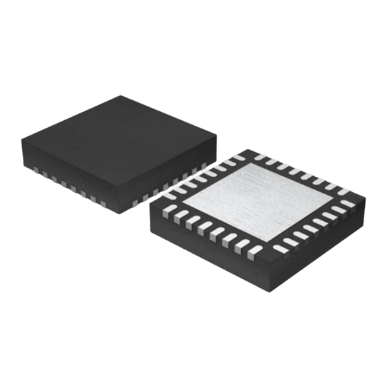
- Page 12 4. The center pad on the QFN package must be connected to ground (Vss) for best mechanical, thermal, and electrical performance. If not connected to ground, it must be electrically floated and not connected to any other signal. Document Number: 38-12025 Rev. *O CY8C21434, CY8C21334, CY8C21234 Description Analog column mux input, integrating input.
- Page 13 P2[7] P2[5] P2[3] P2[1] OCDE OCDO Power Power Power Document Number: 38-12025 Rev. *O CY8C21434, CY8C21334, CY8C21234 Figure 12. CY8C21001 56-Pin PSoC Device AI, P0[7] P0[6], AI AI, P0[5] P0[4], AI AI, P0[3] P0[2], AI AI, P0[1] P0[0], AI P2[7]...
- Page 14 P0[6] Power LEGEND : A = Analog, I = Input, O = Output, and OCD = On-Chip Debug. Document Number: 38-12025 Rev. *O CY8C21634, CY8C21534 CY8C21434, CY8C21334, CY8C21234 Description No connection. No connection. I2C Serial Clock (SCL). I2C Serial Data (SDA).
-
Page 15: Register Reference
PRT2IE PRT2GS PRT2DM2 PRT3DR PRT3IE PRT3GS PRT3DM2 Blank fields are Reserved and must not be accessed. Document Number: 38-12025 Rev. *O CY8C21634, CY8C21534 CY8C21434, CY8C21334, CY8C21234 Table ASE10CR0 ASE11CR0 # Access is bit specific. CUR_PP STK_PP IDX_PP MVR_PP MVW_PP I2C_CFG... - Page 16 PRT1IC1 PRT2DM0 PRT2DM1 PRT2IC0 PRT2IC1 PRT3DM0 PRT3DM1 PRT3IC0 PRT3IC1 Blank fields are Reserved and must not be accessed. Document Number: 38-12025 Rev. *O CY8C21434, CY8C21334, CY8C21234 RDI0RI RDI0SYN RDI0IS RDI0LT0 RDI0LT1 RDI0RO0 RDI0RO1 # Access is bit specific. ASE10CR0 ASE11CR0 # Access is bit specific.
- Page 17 TMP_DR1 DCB03OU TMP_DR2 TMP_DR3 ACE00CR1 ACE00CR2 ACE01CR1 ACE01CR2 Blank fields are Reserved and must not be accessed. Document Number: 38-12025 Rev. *O CY8C21434, CY8C21334, CY8C21234 RDI0RI RDI0SYN RDI0IS RDI0LT0 RDI0LT1 RDI0RO0 RDI0RO1 # Access is bit specific. CY8C21634, CY8C21534 MUX_CR0...
-
Page 18: Electrical Specifications
μH microhenry μs microsecond μV microvolts μVrms microvolts root-mean-square Document Number: 38-12025 Rev. *O CY8C21434, CY8C21334, CY8C21234 ≤ 100 C and T C as specified, except where noted. Figure 14. IMO Frequency Trim Options 5.25 4.75 3.60 3.00 2.40... -
Page 19: Dc Electrical Characteristics
Supply Current, IMO = 24 MHz Supply Current, IMO = 6 MHz using SLIMO mode. Supply Current, IMO = 6 MHz using SLIMO DD27 mode. Document Number: 38-12025 Rev. *O CY8C21434, CY8C21334, CY8C21234 +100 – -0.5 – +6.0 Vss - –... - Page 20 Table 16. 2.7V DC GPIO Specifications Symbol Description Pull up Resistor Pull down Resistor High Output Level Low Output Level Input Low Level Document Number: 38-12025 Rev. *O CY8C21634, CY8C21534 CY8C21434, CY8C21334, CY8C21234 Units μA – μA – 1.28 1.30 1.32 1.16 1.30...
- Page 21 Port 0 Pin 0 is below 1 nA at 25°C; 50 nA over temperature. Use Port 0 Pins 1-7 for the lowest leakage of 200 nA. EBOA Document Number: 38-12025 Rev. *O CY8C21634, CY8C21534 CY8C21434, CY8C21334, CY8C21234 Units – –...
- Page 22 BAT5V Input Voltage Range from Battery BAT3V Input Voltage Range from Battery BAT2V Minimum Input Voltage from Battery to Start BATSTA Pump Document Number: 38-12025 Rev. *O CY8C21434, CY8C21334, CY8C21234 – – – – – Vdd - 1 – –...
- Page 23 PUMP Note 6. L = 2 mH inductor, C = 10 mF capacitor, D = Schottky diode. See Figure 15 Document Number: 38-12025 Rev. *O CY8C21434, CY8C21334, CY8C21234 – – – – – Figure 15. Basic Switch Mode Pump Circuit...
- Page 24 PPOR Always greater than 50 mV above LVD0 Always greater than 50 mV above LVD3 Document Number: 38-12025 Rev. *O CY8C21434, CY8C21334, CY8C21234 ≤ 85°C, or 2.4V to 3.0V and -40°C ≤ T – – – – ≤ 85°C, or 2.4V to 3.0V and -40°C ≤ T 2.36...
- Page 25 50,000 cycles). For the full industrial range, the user must employ a temperature sensor user module (FlashTemp) and feed the result to the temperature argument before writing. Refer to the Flash APIs Application Note information. Document Number: 38-12025 Rev. *O CY8C21434, CY8C21334, CY8C21234 ≤ 85°C, or 2.4V to 3.0V and -40°C ≤ T 2.70 –...
-
Page 26: Ac Electrical Characteristics
AN2012 operation at 3.3V. 15. See the individual user module data sheets for information on maximum frequencies for user modules. Document Number: 38-12025 Rev. *O CY8C21434, CY8C21334, CY8C21234 ≤ 85°C, or 2.4V to 3.0V and -40°C ≤ T [12,13,14] 23.4 24.6... - Page 27 17. Accuracy derived from Internal Main Oscillator with appropriate trim for Vdd range. 18. See Application Note AN2012 “Adjusting PSoC Microcontroller Trims for Dual Voltage-Range Operation” for information on maximum frequency for user modules. Document Number: 38-12025 Rev. *O CY8C21634, CY8C21534 CY8C21434, CY8C21334, CY8C21234 Units [16,17,18] 11.5 12.7 Trimmed for 2.7V operation using factory trim values.
- Page 28 5V at 25°C and are for design guidance only. Table 30. AC Low Power Comparator Specifications Symbol Description LPC response time RLPC Document Number: 38-12025 Rev. *O CY8C21434, CY8C21334, CY8C21234 ≤ 85°C, or 2.4V to 3.0V and -40°C ≤ T – – – – –...
- Page 29 19. 50 ns minimum input pulse width is based on the input synchronizers running at 12 MHz (84 ns nominal period). Document Number: 38-12025 Rev. *O CY8C21434, CY8C21334, CY8C21234 ≤ 85°C, or 2.4V to 3.0V and -40°C ≤ T –...
- Page 30 Power Up IMO to Switch Note 20. 100 ns minimum input pulse width is based on the input synchronizers running at 12 MHz (84 ns nominal period). Document Number: 38-12025 Rev. *O CY8C21634, CY8C21534 CY8C21434, CY8C21334, CY8C21234 Units 12.7 [20] –...
- Page 31 Data Set up Time to Falling Edge of SCLK SSCLK Data Hold Time from Falling Edge of SCLK HSCLK Frequency of SCLK SCLK Flash Erase Time (Block) ERASEB Document Number: 38-12025 Rev. *O CY8C21434, CY8C21334, CY8C21234 0.093 – 12.3 0.186 – 24.6 41.7 –...
- Page 32 SDA line t = 1000 + 250 = 1250 ns (according to the Standard-Mode I2C-bus specification) before the SCL line is released. rmax SU;DAT Document Number: 38-12025 Rev. *O CY8C21634, CY8C21534 CY8C21434, CY8C21334, CY8C21234 Units – – – –...
- Page 33 Figure 19. Definition for Timing for Fast/Standard Mode on the I LOWI2C HDDATI2C HDSTAI2C HIGHI2C Document Number: 38-12025 Rev. *O CY8C21434, CY8C21334, CY8C21234 C SDA and SCL Pins (Fast Mode not Supported) Standard Mode – SUDATI2C HDSTAI2C SUSTAI2C...
-
Page 34: Packaging Information
PSoC Emulator Pod Dimensions at http://www.cypress.com/design/MR10161. Packaging Dimensions 0.386[9.804] 0.393[9.982] 0.050[1.270] 0.0138[0.350] 0.0192[0.487] Document Number: 38-12025 Rev. *O CY8C21434, CY8C21334, CY8C21234 Figure 20. 16-Pin (150-Mil) SOIC PIN 1 ID DIMENSIONS IN INCHES[MM] MIN. REFERENCE JEDEC MS-012 PACKAGE WEIGHT 0.15gms 0.150[3.810] 0.157[3.987] 0.230[5.842] 0.244[6.197]... - Page 35 CY8C21634, CY8C21534 CY8C21434, CY8C21334, CY8C21234 Figure 22. 28-Pin (210-Mil) SSOP 51-85079 *C Figure 23. 32-Pin (5x5 mm 0.93 MAX) QFN E-PAD X, Y for this product is 3.53 mm, 3.53 mm (+/-0.11 mm) 51-85188 *B Document Number: 38-12025 Rev. *O...
- Page 36 CY8C21634, CY8C21534 CY8C21434, CY8C21334, CY8C21234 Figure 24. 32-Pin (5x5 mm 0.60 MAX) QFN E-PAD X, Y for this product is 3.53 mm, 3.53 mm (+/-0.11 mm) 001-06392 *A Figure 25. 32-Pin (5 X 5 X 0.4MM) QFN (SAWN 1.85 X 2.85 EPAD 001-44368 *A Document Number: 38-12025 Rev.
- Page 37 CY8C21634, CY8C21534 CY8C21434, CY8C21334, CY8C21234 Figure 26. 32-Pin Sawn QFN Package 001-30999 *A Figure 27. 32-Pin Thin Sawn QFN Package 001-42168 *C Important Note For information on the preferred dimensions for mounting QFN packages, see the following Application Note at http://www.amkor.com/products/notes_papers/MLFAppNote.pdf.
-
Page 38: Thermal Impedances
[23] 32 QFN 5x5 mm 0.60 MAX [23] 32 QFN 5x5 mm 0.93 MAX Document Number: 38-12025 Rev. *O CY8C21434, CY8C21334, CY8C21234 Figure 28. 56-Pin (300-Mil) SSOP [22] Typical θ CY8C21634, CY8C21534 51-85062 *C Typical θ Page 38 of 45... - Page 39 24. Higher temperatures may be required based on the solder melting point. Typical temperatures for solder are 220 ± 5 paste. Refer to the solder manufacturer specifications. Document Number: 38-12025 Rev. *O CY8C21634, CY8C21534 CY8C21434, CY8C21334, CY8C21234 [24] Maximum Peak Temperature C with Sn-Pb or 245 ± 5...
- Page 40 ICE Flex-Pod for CY8C29x66 Family ■ Cat-5 Adapter ■ Mini-Eval Programming Board ■ Document Number: 38-12025 Rev. *O CY8C21434, CY8C21334, CY8C21234 110 ~ 240V Power Supply, Euro-Plug Adapter ■ iMAGEcraft C Compiler (Registration Required) ■ ISSP Cable ■ USB 2.0 Cable and Blue Cat-5 Cable ■...
-
Page 41: Third-Party Tools
25. Flex-Pod kit includes a practice flex-pod and a practice PCB, in addition to two flex-pods. 26. Foot kit includes surface mount feet that can be soldered to the target PCB. Document Number: 38-12025 Rev. *O CY8C21434, CY8C21334, CY8C21234 Device Programmers All device programmers can be purchased from the Cypress Online Store. -
Page 42: Ordering Information
27. All Digital IO Pins also connect to the common analog mux. 28. Refer to the section 32-Pin Part Pinout on page 11 for pin differences. Document Number: 38-12025 Rev. *O CY8C21634, CY8C21534 CY8C21434, CY8C21334, CY8C21234 -40°C to +85°C -40°C to +85°C -40°C to +85°C -40°C to +85°C -40°Cto +85°C -40°C to +85°C... - Page 43 Ordering Code Definitions CY 8 C 21 xxx-24xx Document Number: 38-12025 Rev. *O CY8C21434, CY8C21334, CY8C21234 Package Type: Thermal Rating: PX = PDIP Pb-Free C = Commercial SX = SOIC Pb-Free I = Industrial PVX = SSOP Pb-Free E = Extended...
- Page 44 Document History Page Document Title: CY8C21234/CY8C21334/CY8C21434/CY8C21534/CY8C21634 PSoC Document Number: 38-12025 Orig. of Submission Revision ECN No. Change 227340 See ECN 235992 See ECN 248572 See ECN 277832 See ECN 285293 See ECN 301739 See ECN 329104 See ECN 352736 See ECN...
- Page 45 I2C system, provided that the system conforms to the I2C Standard Specification as defined by Philips. All products and company names mentioned in this document may be the trademarks of their respective holders. CY8C21434, CY8C21334, CY8C21234 PSoC Solutions psoc.cypress.com...
Need help?
Do you have a question about the CY8C21234 and is the answer not in the manual?
Questions and answers