Table of Contents
Advertisement
Quick Links
1. Features
XRES Pin to Support In-System Serial Programming (ISSP)
■
and External Reset Control in CY8C24894
Powerful Harvard Architecture Processor
■
M8C Processor Speeds to 24 MHz
❐
Two 8x8 Multiply, 32-Bit Accumulate
❐
Low Power at High Speed
❐
3V to 5.25V Operating Voltage
❐
Industrial Temperature Range: -40°C to +85°C
❐
USB Temperature Range: -10°C to +85°C
❐
Advanced Peripherals (PSoC
■
6 Rail-to-Rail Analog PSoC Blocks Provide:
❐
• Up to 14-Bit ADCs
• Up to 9-Bit DACs
• Programmable Gain Amplifiers
• Programmable Filters and Comparators
4 Digital PSoC Blocks Provide:
❐
• 8 to 32-Bit Timers, Counters, and PWMs
• CRC and PRS Modules
• Full-Duplex UART
• Multiple SPI™ Masters or Slaves
• Connectable to all GPI/O Pins
Complex Peripherals by Combining Blocks
❐
Capacitive Sensing Application Capability
❐
2. Logic Block Diagram
Cypress Semiconductor Corporation
Document Number: 38-12018 Rev. *M
®
PSoC
®
Blocks)
P o r t 7
G l o b a l D i g i t a l I n t e r c o n n e c t
S R A M
1 K
I n t e r r u p t
C o n t r o l l e r
D I G I T A L
D i g i t a l
B l o c k
A r r a y
D i g i t a l
2
C l o c k s
M A C s
•
198 Champion Court
CY8C24094, CY8C24794
CY8C24894, CY8C24994
Programmable System-on-Chip™
Full Speed USB (12 Mbps)
■
Four Uni-Directional Endpoints
❐
One Bi-Directional Control Endpoint
❐
USB 2.0 Compliant
❐
Dedicated 256 Byte Buffer
❐
No External Crystal Required
❐
Flexible On-Chip Memory
■
16K Flash Program Storage 50,000 Erase and Write Cycles
❐
1K SRAM Data Storage
❐
In-System Serial Programming (ISSP)
❐
Partial Flash Updates
❐
Flexible Protection Modes
❐
EEPROM Emulation in Flash
❐
Programmable Pin Configurations
■
25 mA Sink, 10 mA Drive on all GPI/O
❐
Pull Up, Pull Down, High Z, Strong, or Open Drain Drive
❐
Modes on all GPI/O
Up to 48 Analog Inputs on GPI/O
❐
Two 33 mA Analog Outputs on GPI/O
❐
Configurable Interrupt on all GPI/O
❐
Precision, Programmable Clocking
■
Internal ±4% 24 and 48 MHz Oscillator
❐
Internal Oscillator for Watchdog and Sleep
❐
0.25% Accuracy for USB with no External Components
❐
Additional System Resources
■
2
I
C Slave, Master, and Multi-Master to 400 kHz
❐
Watchdog and Sleep Timers
❐
User Configurable Low Voltage Detection
❐
P o r t 5
P o r t 4
P o r t 3
P o r t 2
P o r t 1
G l o b a l A n a l o g I n t e r c o n n e c t
P S o C C O R E
S R O M
F l a s h 1 6 K
C P U C o r e ( M 8 C )
C l o c k S o u r c e s
( I n c l u d e s I M O a n d I L O )
S Y S T E M
A N A L O G
A n a l o g
B l o c k
A r r a y
D e c i m a t o r
P O R a n d L V D
I 2 C
T y p e 2
S y s t e m R e s e t s
S Y S T E M R E S O U R C E S
,
•
San Jose
A n a l o g
P o r t 0
D r i v e r s
S l e e p a n d
W a t c h d o g
S Y S T E M
A n a l o g
R e f .
I n t e r n a l
A n a l o g
V o l t a g e
U S B
I n p u t
R e f .
M u x i n g
CA 95134-1709
•
408-943-2600
Revised February 10, 2009
[+] Feedback
Advertisement
Table of Contents

Related Manuals for Cypress Semiconductor CY8C24094


Summary of Contents for Cypress Semiconductor CY8C24094
- Page 1 Complex Peripherals by Combining Blocks ❐ Capacitive Sensing Application Capability ❐ 2. Logic Block Diagram Cypress Semiconductor Corporation Document Number: 38-12018 Rev. *M CY8C24094, CY8C24794 CY8C24894, CY8C24994 ® PSoC Programmable System-on-Chip™ Full Speed USB (12 Mbps) ■ Four Uni-Directional Endpoints ❐...
- Page 2 Every pin is also capable of generating a system interrupt on high level, low level, and change from last read. Document Number: 38-12018 Rev. *M CY8C24094, CY8C24794 CY8C24894, CY8C24994 3.2 The Digital System The Digital System is composed of four digital PSoC blocks.
- Page 3 CT (Continuous Time) and two SC (Switched Capacitor) blocks, as shown in Figure 3-2. Document Number: 38-12018 Rev. *M CY8C24094, CY8C24794 CY8C24894, CY8C24994 Figure 3-2. Analog System Block Diagram A ll IO ( E x c e p t P o r t 7 )
-
Page 4: Getting Started
For assistance with technical issues, search KnowledgeBase articles and forums at www.cypress.com/support. If you cannot Bytes find an answer to your question, call technical support at 1-800-541-4736. Bytes Bytes Bytes Bytes CY8C24094, CY8C24794 CY8C24894, CY8C24994 PSoC designs. They located Page 4 of 47 here: [+] Feedback... -
Page 5: Development Tools
PSoC devices. Emulation pods for each device family are available separately. The emulation pod takes the place of the PSoC device in the target board and performs full speed (24 MHz) operation. CY8C24094, CY8C24794 CY8C24894, CY8C24994 Page 5 of 47 [+] Feedback... - Page 6 Document Number: 38-12018 Rev. *M CY8C24094, CY8C24794 CY8C24894, CY8C24994 6.3 Organize and Connect You can build signal chains at the chip level by interconnecting...
-
Page 7: Document Conventions
Programmable System-on-Chip™ pulse width modulator switched capacitor SRAM static random access memory Document Number: 38-12018 Rev. *M CY8C24094, CY8C24794 CY8C24894, CY8C24994 7.2 Units of Measure A units of measure table is located in the Electrical Specifications section. Table 10-1 on page 20 lists all the abbreviations used to measure the PSoC devices. -
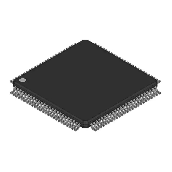
Page 8: Pin Information
I, M P2[2] Direct switched capacitor block input. P2[4] External Analog Ground (AGND) input. Document Number: 38-12018 Rev. *M CY8C24094, CY8C24794 CY8C24894, CY8C24994 Table 8-2 on page 9. Figure 8-1. CY8C24794 56-Pin PSoC Device A, I, M , P2[3] A, I, M , P2[1]... -
Page 9: M, P4[5]
2. The center pad on the QFN package should be connected to ground (Vss) for best mechanical, thermal, and electrical performance. If not connected to ground, it should be electrically floated and not connected to any other signal. Document Number: 38-12018 Rev. *M CY8C24094, CY8C24794 CY8C24894, CY8C24994 Figure 8-2. CY8C24894 56-Pin PSoC Device... -
Page 10: M, P4[3]
P4[0] P4[2] P4[4] LEGENDA = Analog, I = Input, O = Output, NC = No Connection, M = Analog Mux Input. Document Number: 38-12018 Rev. *M CY8C24094, CY8C24794 CY8C24894, CY8C24994 Figure 8-3. CY8C24994 68-Pin PSoC Device M, P4[7] M, P4[5]... -
Page 11: M, P4[1]
8.1 68-Pin Part Pinout (On-Chip Debug) The 68-pin QFN part table and drawing below is for the CY8C24094 On-Chip Debug (OCD) PSoC device. Note This part is only used for in-circuit debugging. It is NOT available for production. Table 8-4. 68-Pin Part Pinout (QFN... -
Page 12: Ocde
External Analog Ground (AGND) input. P4[4] P3[6] No connection. LEGENDA = Analog, I = Input, O = Output, M = Analog Mux Input, NC = No Connection. Document Number: 38-12018 Rev. *M CY8C24094, CY8C24794 CY8C24894, CY8C24994 Name Description No connection. P5[7]... - Page 13 Figure 8-5. CY8C24094 OCD (Not for Production) 8.1 100-Ball VFBGA Part Pinout (On-Chip Debug) The 100-pin VFBGA part table and drawing below is for the CY8C24094 On-Chip Debug (OCD) PSoC device. Note This part is only used for in-circuit debugging. It is NOT available for production.
- Page 14 P3[6] HCLK OCD high-speed clock output. LEGENDA = Analog, I = Input, O = Output, M = Analog Mux Input, NC = No Figure 8-6. CY8C24094 OCD (Not for Production) Document Number: 38-12018 Rev. *M CY8C24094, CY8C24794 CY8C24894, CY8C24994 P3[2]...
- Page 15 8.1 100-Pin Part Pinout (On-Chip Debug) The 100-pin TQFP part is for the CY8C24094 On-Chip Debug (OCD) PSoC device. Note This part is only used for in-circuit debugging. It is NOT available for production. Table 8-7. 100-Pin Part Pinout (TQFP)
- Page 16 Table 8-7. 100-Pin Part Pinout (TQFP) (continued) LEGENDA = Analog, I = Input, O = Output, NC = No Connection, M = Analog Mux Input, OCD = On-Chip Debugger. Figure 8-7. CY8C24094 OCD (Not for Production) AI, M , P0[1]...
-
Page 17: Register Reference
Logical register or bit(s) Clearable register or bit(s) Access is bit specific Document Number: 38-12018 Rev. *M CY8C24094, CY8C24794 CY8C24894, CY8C24994 9.2 Register Mapping Tables The PSoC device has a total register address space of 512 bytes. The register space is referred to as I/O space and is divided into two banks. - Page 18 DCB03CR0 TMP_DR3 ACB00CR3 ACB00CR0 ACB00CR1 ACB00CR2 ACB01CR3 ACB01CR0 ACB01CR1 ACB01CR2 Blank fields are Reserved and should not be accessed. Document Number: 38-12018 Rev. *M CY8C24094, CY8C24794 CY8C24894, CY8C24994 Addr (0,Hex) Access Name Addr (0,Hex) ASC10CR0 ASC10CR1 ASC10CR2 ASC10CR3 ASD11CR0 ASD11CR1...
- Page 19 TMP_DR3 ACB00CR3 ACB00CR0 ACB00CR1 ACB00CR2 ACB01CR3 ACB01CR0 ACB01CR1 ACB01CR2 Blank fields are Reserved and should not be accessed. Document Number: 38-12018 Rev. *M CY8C24094, CY8C24794 CY8C24894, CY8C24994 Addr (1,Hex) Access Name Addr (1,Hex) ASC10CR0 ASC10CR1 ASC10CR2 ASC10CR3 ASD11CR0 ASD11CR1 ASD11CR2...
-
Page 20: Electrical Specifications
Symbol Unit of Measure μW microwatts milli-ampere milli-second milli-volts nanoampere nanosecond nanovolts picoampere picofarad peak-to-peak parts per million picosecond samples per second sigma: one standard deviation volts CY8C24094, CY8C24794 CY8C24894, CY8C24994 http://www.cypress.com/psoc. 24 MHz Page 20 of 47 [+] Feedback... - Page 21 Table 10-3. Operating Temperature Symbol Description Ambient Temperature Ambient Temperature using USB AUSB Junction Temperature Document Number: 38-12018 Rev. *M CY8C24094, CY8C24794 CY8C24894, CY8C24994 Units +100 Higher storage temperatures reduces data retention time. Recom- mended storage temperature is storage temperatures above 65 degrades reliability.
- Page 22 3. Standby current includes all functions (POR, LVD, WDT, Sleep Time) needed for reliable system operation. This should be compared with devices that have similar functions enabled. Document Number: 38-12018 Rev. *M CY8C24094, CY8C24794 CY8C24894, CY8C24994 ≤ 85°C, respectively. Typical parameters apply to 5V and 3.3V at 25°C and Units –...
- Page 23 Power = Low, Opamp Bias = High Power = Medium, Opamp Bias = High Power = High, Opamp Bias = High Document Number: 38-12018 Rev. *M CY8C24094, CY8C24794 CY8C24894, CY8C24994 ≤ 85°C, respectively. Typical parameters apply to 5V and 3.3V at 25°C and Units –...
- Page 24 Table 10-8. DC Low Power Comparator Specifications Symbol Description Low power comparator (LPC) reference REFLPC voltage range LPC supply current SLPC LPC voltage offset OSLPC Document Number: 38-12018 Rev. *M CY8C24094, CY8C24794 CY8C24894, CY8C24994 Units Vdd - – – – – Vdd - – –...
- Page 25 Supply Current Including Bias Cell (No Load) Power = Low Power = High PSRR Supply Voltage Rejection Ratio Document Number: 38-12018 Rev. *M CY8C24094, CY8C24794 CY8C24894, CY8C24994 ≤ 85°C, respectively. Typical parameters apply to 5V and 3.3V at 25°C and Units – μV/°C –...
- Page 26 BG - 0.009 1.6 x BG - 0.027 -0.034 Not Allowed Not Allowed Not Allowed Not Allowed 0.075 CY8C24094, CY8C24794 CY8C24894, CY8C24994 1.30 1.32 Vdd/2 - 0.01 Vdd/2 + 0.007 2 x BG - 0.030 2 x BG + 0.024 P2[4] P2[4] + 0.011...
- Page 27 5. Avoid using P2[4] for digital signaling when using an analog resource that depends on the Analog Reference. Some coupling of the digital signal may appear on the AGND. Document Number: 38-12018 Rev. *M CY8C24094, CY8C24794 CY8C24894, CY8C24994 Not Allowed...
- Page 28 6. Always greater than 50 mV above PPOR (PORLEV = 00) for falling supply. 7. Always greater than 50 mV above PPOR (PORLEV = 10) for falling supply. Document Number: 38-12018 Rev. *M CY8C24094, CY8C24794 CY8C24894, CY8C24994 ≤ 85°C, respectively. Typical parameters apply to 5V or 3.3V at 25°C and are Units 2.91...
- Page 29 For the full industrial range, the user must employ a temperature sensor user module (FlashTemp) and feed the result to the temperature argument before writing. Refer to the Flash APIs Application Note AN2015 at http://www.cypress.com under Application Notes for more information. Document Number: 38-12018 Rev. *M CY8C24094, CY8C24794 CY8C24894, CY8C24994 ≤ 85°C, respectively. Typical parameters apply to 5V and 3.3V at 25°C and Units –...
- Page 30 3.3V. 12. See the individual user module data sheets for information on maximum frequencies for user modules Document Number: 38-12018 Rev. *M CY8C24094, CY8C24794 CY8C24894, CY8C24994 ≤ 85°C, respectively. Typical parameters apply to 5V and 3.3V at 25°C and...
-
Page 31: Document Number: 38-12018 Rev. *M
– – – 12 - 12 + 0.25% 0.25% CY8C24094, CY8C24794 CY8C24894, CY8C24994 Units Notes Normal Strong Mode Vdd = 4.5 to 5.25V, 10% - 90% Vdd = 4.5 to 5.25V, 10% - 90% Vdd = 3 to 5.25V, 10% - 90% Vdd = 3 to 5.25V, 10% - 90%... -
Page 32: Document Number: 38-12018 Rev. *M
Power = Medium, Opamp Bias = High Noise at 1 kHz (Power = Medium, Opamp Bias = High) – Document Number: 38-12018 Rev. *M CY8C24094, CY8C24794 CY8C24894, CY8C24994 ≤ 85°C, respectively. Typical parameters apply to 5V and 3.3V at 25°C and –... -
Page 33: Document Number: 38-12018 Rev. *M
10000 1000 0.001 Document Number: 38-12018 Rev. *M 0.01 Freq (kHz) Figure 10-5. Typical Opamp Noise 0.01 Freq (kHz) CY8C24094, CY8C24794 CY8C24894, CY8C24994 0.01 PH_BH PH_BL PM_BL PL_BL Page 33 of 47 [+] Feedback... -
Page 34: Document Number: 38-12018 Rev. *M
13. 50 ns minimum input pulse width is based on the input synchronizers running at 24 MHz (42 ns nominal period). Document Number: 38-12018 Rev. *M CY8C24094, CY8C24794 CY8C24894, CY8C24994 ≤ 85°C, or 2.4V to 3.0V and -40°C ≤ T Units μs... -
Page 35: Document Number: 38-12018 Rev. *M
– – 0.65 – – , 3dB BW, – – – – , 3dB BW, 100 – – – – CY8C24094, CY8C24794 CY8C24894, CY8C24994 Units Notes μs Units Notes μs μs μs μs V/μs V/μs V/μs V/μs Page 35 of 47... -
Page 36: Document Number: 38-12018 Rev. *M
≤ 85°C, respectively. Typical parameters apply to 5V and 3.3V at 25°C and – – – – – – – – – – – – – – – CY8C24094, CY8C24794 CY8C24894, CY8C24994 Units Notes μs μs μs μs V/μs V/μs V/μs V/μs Units Notes Vdd > 3.6 3.0 ≤ Vdd ≤ 3.6... -
Page 37: Document Number: 38-12018 Rev. *M
C SDA and SCL Pins for Vdd Standard Mode Fast Mode – – – – – [14] – – – – – HDSTAI2C SUSTAI2C SU;DAT CY8C24094, CY8C24794 CY8C24894, CY8C24994 Units Notes μs – μs – μs – μs – μs – – μs –... -
Page 38: Document Number: 38-12018 Rev. *M
Important Note Emulation tools may require a larger area on the target PCB than the chip’s footprint. For a detailed description of the emulation tools’ dimensions, refer to the document titled PSoC Emulator Pod Dimensions at http://www.cypress.com/design/MR10161. Document Number: 38-12018 Rev. *M CY8C24094, CY8C24794 CY8C24894, CY8C24994 Figure 11-1. 56-Pin (8x8 mm) QFN 001-12921 **... -
Page 39: Document Number: 38-12018 Rev. *M
Pinned vias for thermal conduction are not required for the low-power PSoC device. ■ Figure 11-3. 68-Pin SAWN QFN (8X8 mm X 0.90 mm) Document Number: 38-12018 Rev. *M Figure 11-2. 68-Pin (8x8 mm x 0.89 mm) QFN CY8C24094, CY8C24794 CY8C24894, CY8C24994 51-85214 *C 001-09618 *A Page 39 of 47... -
Page 40: Document Number: 38-12018 Rev. *M
CY8C24094, CY8C24794 CY8C24894, CY8C24994 Figure 11-4. 100-Ball (6x6 mm) VFBGA 51-85209 *B Figure 11-5. 100-Pin (14x14 x 1.4 mm) TQFP 51-85048 *C Document Number: 38-12018 Rev. *M Page 40 of 47 [+] Feedback... -
Page 41: Document Number: 38-12018 Rev. *M
16. To achieve the thermal impedance specified for the QFN package, the center thermal pad should be soldered to the PCB ground plane. 17. Higher temperatures may be required based on the solder melting point. Typical temperatures for solder are 220 ± 5 Refer to the solder manufacturer specifications Document Number: 38-12018 Rev. *M CY8C24094, CY8C24794 CY8C24894, CY8C24994 [15] [17] Maximum Peak Temperature C with Sn-Pb or 245 ±... -
Page 42: Document Number: 38-12018 Rev. *M
Cat-5 Adapter ■ Mini-Eval Programming Board ■ 110 ~ 240V Power Supply, Euro-Plug Adapter ■ Document Number: 38-12018 Rev. *M CY8C24094, CY8C24794 CY8C24894, CY8C24994 iMAGEcraft C Compiler (Registration Required) ■ ISSP Cable ■ USB 2.0 Cable and Blue Cat-5 Cable ■... -
Page 43: Document Number: 38-12018 Rev. *M
20. Programming adapter converts non-DIP package to DIP footprint. Specific details and ordering information for each of the adapters are found at http://www.emulation.com. Document Number: 38-12018 Rev. *M CY8C24094, CY8C24794 CY8C24894, CY8C24994 12.4 Device Programmers All device programmers can be purchased from the Cypress Online Store. -
Page 44: Document Number: 38-12018 Rev. *M
CY8C24094-24LTXI 68-Pin QFN (Sawn) CY8C24094-24LTXIT Note For Die sales information, contact a local Cypress sales office or Field Applications Engineer (FAE). Document Number: 38-12018 Rev. *M CY8C24094, CY8C24794 CY8C24894, CY8C24994 -40°C to +85°C -40°C to +85°C -40°C to +85°C -40°C to +85°C -40°C to +85°C... -
Page 45: Document Number: 38-12018 Rev. *M
13.1 Ordering Code Definitions 8 C 24 XXX- SP XX Note 21. This part may be used for in-circuit debugging. It is NOT available for production. Document Number: 38-12018 Rev. *M CY8C24094, CY8C24794 CY8C24894, CY8C24994 Package Type: Thermal Rating: PX = PDIP Pb-Free... -
Page 46: Document Number: 38-12018 Rev. *M
14. Document History Page Document Title: CY8C24094, CY8C24794, CY8C24894 and CY8C24994 PSoC® Programmable System-on-Chip™ Document Number: 38-12018 ECN No. Submission Orig. of Rev. Date Change 133189 01.27.2004 251672 See ECN 289742 See ECN 335236 See ECN 344318 See ECN 346774... -
Page 47: Document Number: 38-12018 Rev. *M
PSoC Solutions psoc.cypress.com General clocks.cypress.com Low Power/Low Voltage Precision Analog LCD Drive image.cypress.com CAN 2.0b Revised February 10, 2009 CY8C24094, CY8C24794 CY8C24894, CY8C24994 psoc.cypress.com/solutions psoc.cypress.com/low-power psoc.cypress.com/precision-analog psoc.cypress.com/lcd-drive psoc.cypress.com/can psoc.cypress.com/usb Page 47 of 47 [+] Feedback...
Need help?
Do you have a question about the CY8C24094 and is the answer not in the manual?
Questions and answers