Table of Contents
Advertisement
Quick Links
Features
■
Powerful Harvard Architecture Processor
❐
M8C Processor Speeds to 24 MHz
❐
8x8 Multiply, 32-Bit Accumulate
❐
Low Power at High Speed
❐
3.0 to 5.25V Operating Voltage
❐
Industrial Temperature Range: -40°C to +85°C
■
Advanced Peripherals (PSoC Blocks)
❐
4 Rail-to-Rail analog PSoC Blocks Provide:
• Up to 14-Bit ADCs
• Up to 8-Bit DACs
• Programmable Gain Amplifiers
• Programmable Filters and Comparators
❐
4 Digital PSoC Blocks Provide:
• 8 to 32-Bit Timers, Counters, and PWMs
• CRC and PRS Modules
• Full-Duplex UART
• Multiple SPI™ Masters or Slaves
• Connectable to All GPIO Pins
❐
Complex Peripherals by Combining Blocks
❐
High-Speed 8-Bit SAR ADC Optimized for Motor Control
■
Precision, Programmable Clocking
❐
Internal ±2.5% 24/48 MHz Oscillator
❐
High Accuracy 24 MHz with Optional 32 kHz Crystal and PLL
❐
Optional External Oscillator, up to 24 MHz
❐
Internal Oscillator for Watchdog and Sleep
■
Flexible On-Chip Memory
❐
8K Bytes Flash Program Storage 50,000 Erase/Write Cycles
❐
256 Bytes SRAM Data Storage
❐
In-System Serial Programming (ISSP)
❐
Partial Flash Updates
❐
Flexible Protection Modes
❐
EEPROM Emulation in Flash
■
Programmable Pin Configurations
❐
25 mA Sink on all GPIO
❐
Pull up, Pull Down, High Z, Strong, or Open Drain Drive
Modes on All GPIO
❐
Up to Ten Analog Inputs on GPIO
❐
Two 30 mA Analog Outputs on GPIO
❐
Configurable Interrupt on All GPIO
■
Additional System Resources
2
❐
I
C™ Slave, Master, and Multi-Master to 400 kHz
❐
Watchdog and Sleep Timers
❐
User-Configurable Low Voltage Detection
❐
Integrated Supervisory Circuit
❐
On-chip Precision Voltage Reference
Cypress Semiconductor Corporation
Document Number: 001-44369 Rev. *B
®
PSoC
Programmable System-on-Chip™
■
Complete Development Tools
❐
Free Development Software (PSoC Designer™)
❐
Full-Featured In-Circuit Emulator and Programmer
❐
Full Speed Emulation
❐
Complex Breakpoint Structure
❐
128K Bytes Trace Memory
Logic Block Diagram
•
198 Champion Court
CY8C23433, CY8C23533
Port 3
Port 2
PSoC CORE
System Bus
Global Digital Interconnect
Global Analog Interconnect
SRAM
SROM
Flash 8K
256 Bytes
CPU Core (M8C)
Interrupt
Controller
Multiple Clock Sources
(Includes IMO, ILO, PLL, and ECO)
DIGITAL SYSTEM
ANALOG SYSTEM
Digital
Analog
Block
Block Array
Array
2 Columns
4 Blocks
1 Row
4 Blocks
SAR8 ADC
Digital
Multiply
Decimator
2
I
C
Clocks
Accum.
SYSTEM RESOURCES
,
•
San Jose
CA 95134-1709
Revised December 05, 2008
Analog
Port 1 Port 0
Drivers
Sleep and
Watchdog
Analog
Ref
Analog
Input
Muxing
Internal
POR and LVD
Voltage
System Resets
Ref.
•
408-943-2600
[+] Feedback
Advertisement
Table of Contents

Subscribe to Our Youtube Channel
Related Manuals for Cypress Semiconductor CY8C23533


Summary of Contents for Cypress Semiconductor CY8C23533
- Page 1 Array 1 Row 4 Blocks Digital Multiply Clocks Accum. • 198 Champion Court • San Jose CY8C23433, CY8C23533 Analog Port 3 Port 2 Port 1 Port 0 Drivers Global Analog Interconnect SROM Flash 8K CPU Core (M8C) Sleep and Watchdog...
-
Page 2: Digital System
Document Number: 001-44369 Rev. *B CY8C23433, CY8C23533 Digital System The Digital System consists of 4 digital PSoC blocks. Each block is an 8-bit resource that is used alone or combined with other blocks to form 8, 16, 24, and 32-bit peripherals, which are called user module references. -
Page 3: Analog System
CT (Continuous Time) and two SC (Switched Capacitor) blocks. The Analog Column 0 contains the SAR8 ADC block rather than the standard SC blocks. Document Number: 001-44369 Rev. *B CY8C23433, CY8C23533 Figure 2. Analog System Block Diagram P0[7] P0[5]... -
Page 4: Getting Started
Application Notes A long list of application notes can assist you in every aspect of your design effort. To view the PSoC application notes, go to http://www.cypress.com/psocapnotes. CY8C23433, CY8C23533 and select Application Notes CapSense. http://www.cypress.com, click on Design... -
Page 5: Development Tools
C tailored to the PSoC architecture. It comes complete with embedded libraries providing port and bus operations, standard keypad and display support, and extended math functionality. Device Programmer CY8C23433, CY8C23533 dynamic reconfiguration. Dynamic Page 5 of 37 [+] Feedback... -
Page 6: Hardware Tools
For example, a Pulse Width Modulator User Module configures one or more digital PSoC blocks, one for each 8 bits Document Number: 001-44369 Rev. *B CY8C23433, CY8C23533 of resolution. The user module parameters permit you to establish the pulse width and duty cycle. User modules also provide tested software to cut your development time. -
Page 7: Document Conventions
‘3Ah’). Hexadecimal numbers may also be represented by a ‘0x’ prefix, the C coding convention. Binary numbers have an appended lowercase ‘01000011b’). Numbers not indicated by an ‘h’ or ‘b’ are decimal. CY8C23433, CY8C23533 Description Electrical Table 8 on page 14 lists all the ‘b’... - Page 8 LEGEND : A = Analog, I = Input, and O = Output. Note 4. Even though P3[0] is an odd port, it resides on the left side of the pinout. Document Number: 001-44369 Rev. *B CY8C23433, CY8C23533 Figure 5. CY8C23533 32-Pin PSoC Device Description GPIO, P2[7] GPIO, P2[5] A, I, P2[3]...
- Page 9 6. ISSP pin, which is not High Z at POR. 7. Even though P3[1] is an even port, it resides on the right side of the pinout. Document Number: 001-44369 Rev. *B CY8C23433, CY8C23533 Figure 6. CY8C23433 28-Pin PSoC Device AIO, P0[7]...
-
Page 10: Register Reference
Clearable register or bits Access is bit specific Document Number: 001-44369 Rev. *B CY8C23433, CY8C23533 Register Mapping Tables The PSoC device has a total register address space of 512 bytes. The register space is referred to as IO space and is divided into two banks. - Page 11 DCB03CR0 TMP_DR3 ACB00CR3 ACB00CR0 ACB00CR1 ACB00CR2 ACB01CR3 ACB01CR0 ACB01CR1 * ACB01CR2 * Gray fields are reserved. # Access is bit specific. Document Number: 001-44369 Rev. *B CY8C23433, CY8C23533 ASD11CR0 ASD11CR1 ASD11CR2 ASD11CR3 ASC21CR0 ASC21CR1 ASC21CR2 ASC21CR3 RDI0RI RDI0SYN RDI0IS RDI0LT0...
- Page 12 (continued) ASD11CR0 ASD11CR1 ASD11CR2 ASD11CR3 ASC21CR0 ASC21CR1 ASC21CR2 ASC21CR3 SARADC_TRS SARADC_TRCL SARADC_TRCH SARADC_CR2 SARADC_LCR RDI0RI RDI0SYN RDI0IS RDI0LT0 RDI0LT1 CY8C23433, CY8C23533 CPU_SCR1 CPU_SCR0 GDI_O_IN GDI_E_IN GDI_O_OU GDI_E_OU OSC_GO_EN OSC_CR4 OSC_CR3 OSC_CR0 OSC_CR1 OSC_CR2 VLT_CR VLT_CMP IMO_TR ILO_TR BDG_TR ECO_TR Page 12 of 37...
- Page 13 Table 7. Register Map Bank 1 Table: Configuration Space (continued) ACB01CR0 ACB01CR1 ACB01CR2 * Gray fields are reserved. # Access is bit specific. Document Number: 001-44369 Rev. *B CY8C23433, CY8C23533 RDI0RO0 RDI0RO1 CPU_F FLS_PR1 CPU_SCR1 CPU_SCR0 Page 13 of 37...
-
Page 14: Electrical Specifications
Document Number: 001-44369 Rev. *B ≤ 85°C and T 5.25 4.75 3.60 3.00 12 MHz 24 MHz Symbol μW CY8C23433, CY8C23533 ≤ 100°C, except where noted. Refer to Figure 8. IMO Frequency Trim Options SLIMO SLIMO Mode=1 Mode=0 SLIMO SLIMO Mode=0... -
Page 15: Absolute Maximum Ratings
Latch-up Current Operating Temperature Table 10. Operating Temperature Symbol Description Ambient Temperature Junction Temperature Document Number: 001-44369 Rev. *B CY8C23433, CY8C23533 Units +100 °C Higher storage temperatures reduce data retention time. Recommended storage temperature is +25°C ± 25°C. Extended duration storage temperatures above 65°C... -
Page 16: Dc Electrical Characteristics
– – – – – – 1.28 1.30 1.33 CY8C23433, CY8C23533 Units Notes DC POR and LVD Specifications on page 22. Conditions are Vdd = 5.0V, = 25°C, CPU = 3 MHz, SYSCLK doubler disabled, VC1 = 1.5 MHz, VC2 = 93.75 kHz, VC3 = 93.75 kHz,... - Page 17 Input Hysterisis Input Leakage (Absolute Value) Capacitive Load on Pins as Input Capacitive Load on Pins as Output Document Number: 001-44369 Rev. *B CY8C23433, CY8C23533 ≤ 85°C, respectively. Typical parameters apply to 5V and 3.3V at 25°C and Units kΩ kΩ...
- Page 18 Power = High, Opamp Bias = Low Power = High, Opamp Bias = High PSRR Supply Voltage Rejection Ratio Document Number: 001-44369 Rev. *B CY8C23433, CY8C23533 ≤ 85°C, respectively. Typical parameters apply to 5V and 3.3V at 25°C and Units – –...
- Page 19 Table 15. DC Low Power Comparator Specifications Symbol Description Low power comparator (LPC) reference voltage REFLPC range LPC supply current SLPC LPC voltage offset OSLPC Document Number: 001-44369 Rev. *B CY8C23433, CY8C23533 Units – 1.65 – 1.32 μV/°C – 35.0 – –...
- Page 20 Supply Current Including Bias Cell (No Load) Power = Low Power = High PSRR Supply Voltage Rejection Ratio Document Number: 001-44369 Rev. *B CY8C23433, CY8C23533 ≤ 85°C, respectively. Typical parameters apply to 5V and 3.3V at 25°C and – – – Vdd - 1.0 –...
- Page 21 – RefHi = Vdd/2 + BandGap – RefHi = 3 x BandGap Document Number: 001-44369 Rev. *B CY8C23433, CY8C23533 ≤ 85°C, respectively. Typical parameters apply to 5V and 3.3V at 25°C and 1.28 1.30 Vdd/2 - 0.04 Vdd/2 - 0.01 2 x BG - 0.048...
- Page 22 10. Always greater than 50 mV above V (PORLEV=01) for falling supply. PPOR Document Number: 001-44369 Rev. *B CY8C23433, CY8C23533 Not Allowed Not Allowed P2[4] + P2[6] - 0.075 P2[4] + P2[6] - 0.009...
- Page 23 – Vss + 0.75 Vdd - 1.0 – 50,000 – 1,800,000 – – http://www.cypress.com under Application Notes for more information. CY8C23433, CY8C23533 Units Notes – – Driving internal pull down resistor Driving internal pull down resistor – – Erase/write cycles per block –...
- Page 24 12. SAR converters require a stable input voltage during the sampling period. If the voltage into the SAR8 changes by more than 1 LSB during the sampling period then the accuracy specifications may not be met Document Number: 001-44369 Rev. *B CY8C23433, CY8C23533 ≤ 85°C, respectively. Typical parameters apply to 5V and 3.3V at 25°C and Units –...
-
Page 25: Ac Electrical Characteristics
49.2 – – – – – “Adjusting PSoC Microcontroller Trims for Dual Voltage-Range Operation” for information on trimming for operation CY8C23433, CY8C23533 Units Notes MHz Trimmed for 5V or 3.3V operation using factory trim values. See Figure 8 on page 14. - Page 26 Figure 12. 24 MHz Period Jitter (IMO) Timing Diagram Figure 13. 32 kHz Period Jitter (ECO) Timing Diagram 32K2 Document Number: 001-44369 Rev. *B Figure 9. PLL Lock Timing Diagram PLLSLEW PLLSLEWLOW Jitter24M1 Jitter32k CY8C23433, CY8C23533 24 MHz 24 MHz 32 kHz Page 26 of 37 [+] Feedback...
- Page 27 TFallF TRiseS TFallS ≤ 85°C, respectively. Typical parameters apply to 5V and 3.3V at 25°C and Description CY8C23433, CY8C23533 Units Notes Normal Strong Mode Vdd = 4.5 to 5.25V, 10% - 90% Vdd = 4.5 to 5.25V, 10% - 90% Vdd = 3 to 5.25V, 10% - 90%...
- Page 28 Power = Low, Opamp Bias = Low Power = Medium, Opamp Bias = High Gain Bandwidth Product Power = Low, Opamp Bias = Low Power = Medium, Opamp Bias = High Document Number: 001-44369 Rev. *B Description CY8C23433, CY8C23533 Units μs – – 3.92 μs –...
- Page 29 10000 1000 0.001 Document Number: 001-44369 Rev. *B 0.01 Freq (kHz) Figure 16. Typical Opamp Noise 0.01 Freq (kHz) CY8C23433, CY8C23533 0.01 PH_BH PH_BL PM_BL PL_BL Page 29 of 37 [+] Feedback...
- Page 30 17. 50 ns minimum input pulse width is based on the input synchronizers running at 24 MHz (42 ns nominal period). Document Number: 001-44369 Rev. *B CY8C23433, CY8C23533 ≤ 85°C, respectively. Typical parameters apply to 5V and 3.3V at 25°C and Units μs...
- Page 31 ≤ 85°C, respectively. Typical parameters apply to 5V and 3.3V at 25°C and , 3 dB BW, 100 pF Load , 3 dB BW, 100 pF Load , 3 dB BW, 100 pF Load , 3 dB BW, 100 pF Load CY8C23433, CY8C23533 – – – –...
- Page 32 ≤ 85°C, respectively. Typical parameters apply to 5V and 3.3V at 25°C and – – – – ≤ 85°C, respectively. Typical parameters apply to 5V and 3.3V at 25°C and [20] CY8C23433, CY8C23533 – 24.6 20.6 – 5300 20.6 –...
- Page 33 C SDA and SCL Pins for Vdd > 3.0V Standard Mode C SDA and SCL Pins for Vdd < 3.0V (Fast Mode Not Supported) Standard Mode SUDATI2C HDSTAI2C SUSTAI2C HIGHI2C SU;DAT Figure 18. CY8C23433, CY8C23533 Fast Mode – – – – – – – –...
-
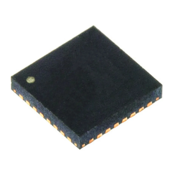
Page 34: Packaging Information
2. BASED ON REF JEDEC # MO-248 3. PACKAGE WEIGHT: 0.0388g 4. DIMENSIONS ARE IN MILLIMETERS Document Number: 001-44369 Rev. *B Figure 19. 32-Pin (5x5 mm) QFN SIDE VIEW CY8C23433, CY8C23533 SEE NOTE 1 BOTTOM VIEW CYPRESS COMPANY CONFIDENTIAL TITLE 32L QFN 5 X 5 X 0.55 MM PACKAGE OUTLINE 3.5 X 3.5 EPAD... - Page 35 Table 39. Typical Package Capacitance on Crystal Pins [22] Package 32 QFN 28 SSOP [23] Maximum Peak Temperature 260°C 260°C CY8C23433, CY8C23533 51-85079 *C Package Capacitance 2.0 pF 2.8 pF C with Sn-Pb or 245 ± 5 C with Sn-Ag-Cu paste. Page 35 of 37 [+] Feedback...
-
Page 36: Ordering Information
28 Pin (210 Mil) SSOP CY8C23433-24PVXI 28 Pin (210 Mil) SSOP CY8C23433-24PVXIT (Tape and Reel) Document Number: 001-44369 Rev. *B CY8C23433, CY8C23533 -40°C to +85°C -40°C to +85°C -40°C to +85°C -40°C to +85°C Page 36 of 37 [+] Feedback... - Page 37 Data sheet creation Moved from Preliminary to Final. Part number changed to CY8C23433, CY8C23533. Adjusted placement of the block diagram; updated description of DAC; updated package pinout description, updated POR and LVD spec, Added Csc , Flash Vdd, SAR ADC spec. Updated package diagram 001-42168 to *A.
Need help?
Do you have a question about the CY8C23533 and is the answer not in the manual?
Questions and answers