Table of Contents
Advertisement
Quick Links
Features
• Single 3.3V power supply
• Ideal for low-voltage cache memory applications
• High speed
— 10/12/15 ns
• Low active power
— 216 mW (max.)
• Low-power alpha immune 6T cell
• Plastic SOJ and TSOP packaging
Functional Description
The CY7C1399B is a high-performance 3.3V CMOS Static
RAM organized as 32,768 words by 8 bits. Easy memory ex-
pansion is provided by an active LOW Chip Enable (CE) and
Logic Block Diagram
A
0
A
1
A
2
A
3
A
4
A
5
A
6
A
7
A
8
A
9
CE
WE
OE
Selection Guide
Maximum Access Time (ns)
Maximum Operating Current (mA)
Maximum CMOS Standby Current ( A)
Cypress Semiconductor Corporation
Document #: 38-05071 Rev. *A
INPUT BUFFER
32K x 8
ARRAY
POWER
COLUMN
DOWN
DECODER
L
•
3901 North First Street
32K x 8 3.3V Static RAM
active LOW Output Enable (OE) and three-state drivers. The
device has an automatic power-down feature, reducing the
power consumption by more than 95% when deselected.
An active LOW Write Enable signal (WE) controls the writing/
reading operation of the memory. When CE and WE inputs are
both LOW, data on the eight data input/output pins (I/O
through I/O
) is written into the memory location addressed by
7
the address present on the address pins (A
Reading the device is accomplished by selecting the device
and enabling the outputs, CE and OE active LOW, while WE
remains inactive or HIGH. Under these conditions, the con-
tents of the location addressed by the information on address
pins is present on the eight data input/output pins.
The input/output pins remain in a high-impedance state unless
the chip is selected, outputs are enabled, and Write Enable
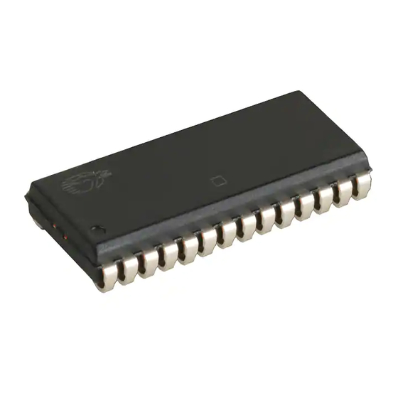
(WE) is HIGH. The CY7C1399B is available in 28-pin standard
300-mil-wide SOJ and TSOP Type I packages.
I/O
0
I/O
1
I/O
2
I/O
3
I/O
4
I/O
5
I/O
6
I/O
7
1399B-10
1399B-12
10
12
60
55
500
500
50
50
•
San Jose
CY7C1399B
through A
0
Pin Configurations
SOJ
Top View
A
V
28
1
5
CC
A
27
WE
2
6
A
26
3
A
7
4
A
4
25
A
8
3
24
A
5
A
9
2
A
23
6
A
10
1
A
22
11
7
OE
A
21
A
12
8
0
A
20
CE
13
9
A
19
10
I/O
14
7
I/O
18
I/O
11
0
6
17
I/O
12
I/O
1
5
13
16
I/O
I/O
2
4
15
I/O
GND
14
3
1399B-15
1399B-20
15
50
500
50
•
CA 95134
•
408-943-2600
Revised June 19, 2001
0
).
14
20
45
500
50
Advertisement
Table of Contents

Related Manuals for Cypress Semiconductor CY7C1399B


Summary of Contents for Cypress Semiconductor CY7C1399B
-
Page 1: Pin Configurations
The input/output pins remain in a high-impedance state unless the chip is selected, outputs are enabled, and Write Enable (WE) is HIGH. The CY7C1399B is available in 28-pin standard 300-mil-wide SOJ and TSOP Type I packages. POWER... -
Page 2: Pin Configuration
, CE V – 0.3V, V – 0.3V, or V 0.3V, WE V – 0.3V or WE 0.3V, f = f CY7C1399B Ambient Temperature 0 C to +70 C 3.3V 300 mV –40 C to +85 C 3.3V 300 mV... - Page 3 Max. V , CE V –0.3V, V – 0.3V, or V 0.3V, WE V –0.3V or WE 0.3V, Description Test Conditions = 25 C, f = 1 MHz, V 1.73V CY7C1399B 1399B-15 1399B-20 Min. Max. Min. Max. +0.3V +0.3V –0.3 –0.3 –1...
-
Page 4: Switching Characteristics
Description [6, 7] [6, 7] is less than t is less than t HZCE LZCE HZOE LZOE and t HZWE CY7C1399B 1399B–10 1399B–12 Min. Max. Min. Max. , and t is less than t for any given device. HZWE LZWE... - Page 5 [6, 7] (Over the Operating Range - L version only) Description Conditions Com’l = 2.0V, CE > V – 0.3V, > V – 0.3V or < 0.3V CY7C1399B 1399B–15 1399B–20 Min. Max. Min. Max. Min. Max. Unit Unit Page 5 of 10...
-
Page 6: Switching Waveforms
10. Device is continuously selected. OE, CE = V 11. WE is HIGH for read cycle. 12. Address valid prior to or coincident with CE transition LOW. Document #: 38-05071 Rev. *A DATA RETENTION MODE 3.0V LZOE CY7C1399B 3.0V DATA VALID HZOE HZCE IMPEDANCE DATA VALID... - Page 7 14. If CE goes HIGH simultaneously with WE HIGH, the output remains in a high-impedance state. 15. During this period, the I/Os are in the output state and input signals should not be applied. Document #: 38-05071 Rev. *A DATA DATA [9, 14] DATA HZWE CY7C1399B VALID VALID VALID LZWE Page 7 of 10...
-
Page 8: Truth Table
Truth Table Input/Output High Z Data Out Data In High Z Ordering Information Speed (ns) Ordering Code CY7C1399B-10VC CY7C1399B-10ZC CY7C1399BL-10VC CY7C1399BL-10ZC CY7C1399B–12VC CY7C1399B–12ZC CY7C1399BL-12VC CY7C1399BL-12ZC CY7C1399B–12VI CY7C1399B–12ZI CY7C1399B–15VC CY7C1399B–15ZC CY7C1399BL-15VC CY7C1399BL-15ZC CY7C1399B–15VI CY7C1399B–15ZI CY7C1399B–20VC CY7C1399B–20ZC CY7C1399BL-20VC CY7C1399BL-20ZC CY7C1399B–20VI CY7C1399B–20ZI Document #: 38-05071 Rev. *A... -
Page 9: Package Diagrams
CY7C1399B Package Diagrams 28-Lead (300-Mil) Molded SOJ V21 51-85031-B 28-Lead Thin Small Outline Package Type 1 (8x13.4 mm) Z28 51-85071-*G Document #: 38-05071 Rev. *A Page 9 of 10 © Cypress Semiconductor Corporation, 2001. The information contained herein is subject to change without notice. Cypress Semiconductor Corporation assumes no responsibility for the use of any circuitry other than circuitry embodied in a Cypress Semiconductor product. -
Page 10: Revision History
Revision History Document Title: CY7C1399B 32K x 8 3.3V Static RAM Document Number: 38-05071 REV. ECN NO. ISSUE DATE 107264 05/25/01 107533 06/28/01 Document #: 38-05071 Rev. *A ORIG. OF CHANGE DESCRIPTION OF CHANGE Change from Spec #: 38-01102 to 38-05071...
Need help?
Do you have a question about the CY7C1399B and is the answer not in the manual?
Questions and answers