Table of Contents
Advertisement
Quick Links
Features
■
18-Mbit density (2M x 8, 2M x 9, 1M x 18, 512K x 36)
■
300 MHz clock for high bandwidth
■
2-word burst for reducing address bus frequency
■
Double Data Rate (DDR) interfaces
(data transferred at 600 MHz) at 300 MHz
■
Two input clocks (K and K) for precise DDR timing
❐
SRAM uses rising edges only
■
Two input clocks for output data (C and C) to minimize clock
skew and flight time mismatches
■
Echo clocks (CQ and CQ) simplify data capture in high-speed
systems
■
Synchronous internally self-timed writes
■
1.8V core power supply with HSTL inputs and outputs
■
Variable drive HSTL output buffers
■
Expanded HSTL output voltage (1.4V–V
■
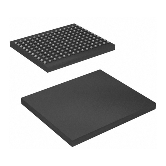
Available in 165-Ball FBGA package (13 x 15 x 1.4 mm)
■
Offered in both Pb-free and non Pb-free packages
■
JTAG 1149.1 compatible test access port
■
Delay Lock Loop (DLL) for accurate data placement
Configurations
CY7C1392BV18 – 2M x 8
CY7C1992BV18 – 2M x 9
CY7C1393BV18 – 1M x 18
CY7C1394BV18 – 512K x 36
Selection Guide
Description
Maximum Operating Frequency
Maximum Operating Current
Cypress Semiconductor Corporation
Document #: 38-05623 Rev. *D
18-Mbit DDR-II SIO SRAM 2-Word
)
DD
300 MHz
278 MHz
300
278
x8
820
770
x9
825
775
x18
865
800
x36
935
850
•
198 Champion Court
CY7C1392BV18, CY7C1992BV18
CY7C1393BV18, CY7C1394BV18
Burst Architecture
Functional Description
The CY7C1392BV18, CY7C1992BV18, CY7C1393BV18, and
CY7C1394BV18 are 1.8V Synchronous Pipelined SRAMs,
equipped with Double Data Rate Separate IO (DDR-II SIO)
architecture. The DDR-II SIO consists of two separate ports: the
read port and the write port to access the memory array. The
read port has data outputs to support read operations and the
write port has data inputs to support write operations. The DDR-II
SIO has separate data inputs and data outputs to completely
eliminate the need to "turn-around" the data bus required with
common IO devices. Access to each port is accomplished
through a common address bus. Addresses for read and write
are latched on alternate rising edges of the input (K) clock. Write
data is registered on the rising edges of both K and K. Read data
is driven on the rising edges of C and C if provided, or on the
rising edge of K and K if C/C are not provided. Each address
location is associated with two 8-bit words in the case of
CY7C1392BV18,
two
9-bit
CY7C1992BV18,
two
18-bit
CY7C1393BV18, and two 36-bit words in the case of
CY7C1394BV18 that burst sequentially into or out of the device.
Asynchronous inputs include an output impedance matching
input (ZQ). Synchronous data outputs are tightly matched to the
two output echo clocks CQ/CQ, eliminating the need to capture
data separately from each individual DDR-II SIO SRAM in the
system design. Output data clocks (C/C) enable maximum
system clocking and data synchronization flexibility.
All synchronous inputs pass through input registers controlled by
the K or K input clocks. All data outputs pass through output
registers controlled by the C or C (or K or K in a single clock
domain) input clocks. Writes are conducted with on-chip
synchronous self-timed write circuitry.
250 MHz
200 MHz
250
200
700
575
700
575
725
600
770
630
,
•
San Jose
CA 95134-1709
words
in
the
case
of
words
in
the
case
of
167 MHz
Unit
167
MHz
485
mA
490
500
540
•
408-943-2600
Revised June 2, 2008
[+] Feedback
Advertisement
Table of Contents

Related Manuals for Cypress Semiconductor CY7C1392BV18


Summary of Contents for Cypress Semiconductor CY7C1392BV18
-
Page 1: Functional Description
■ JTAG 1149.1 compatible test access port ■ Delay Lock Loop (DLL) for accurate data placement Configurations CY7C1392BV18 – 2M x 8 CY7C1992BV18 – 2M x 9 CY7C1393BV18 – 1M x 18 CY7C1394BV18 – 512K x 36 Selection Guide Description... - Page 2 Logic Block Diagram (CY7C1392BV18) [7:0] Address (19:0) Register Gen. DOFF Control Logic [1:0] Logic Block Diagram (CY7C1992BV18) [8:0] Address (19:0) Register Gen. DOFF Control Logic Document #: 38-05623 Rev. *D CY7C1392BV18, CY7C1992BV18 CY7C1393BV18, CY7C1394BV18 Write Write Data Reg Data Reg...
- Page 3 Logic [1:0] Logic Block Diagram (CY7C1394BV18) [35:0] Address (17:0) Register Gen. DOFF Control Logic [3:0] Document #: 38-05623 Rev. *D CY7C1392BV18, CY7C1992BV18 CY7C1393BV18, CY7C1394BV18 Write Write Data Reg Data Reg Control Logic Read Data Reg. Reg. Reg. Reg. Write Write...
-
Page 4: Pin Configuration
Pin Configuration The pin configuration for CY7C1392BV18, CY7C1992BV18, CY7C1393BV18, and CY7C1394BV18 follows. NC/72M DOFF NC/72M DOFF Note 1. NC/36M, NC/72M, NC/144M, and NC/288M are not connected to the die and can be tied to any voltage level. Document #: 38-05623 Rev. *D... - Page 5 Pin Configuration (continued) The pin configuration for CY7C1392BV18, CY7C1992BV18, CY7C1393BV18, and CY7C1394BV18 follows. NC/144M NC/36M DOFF NC/288M NC/72M DOFF Document #: 38-05623 Rev. *D CY7C1392BV18, CY7C1992BV18 CY7C1393BV18, CY7C1394BV18 165-Ball FBGA (13 x 15 x 1.4 mm) Pinout CY7C1393BV18 (1M x 18)
-
Page 6: Pin Definitions
Synchronous 2M x 8 (2 arrays each of 1M x 8) for CY7C1392BV18, 2M x 9 (2 arrays each of 1M x 9) for CY7C1992BV18, 1M x 18 (2 arrays each of 512K x 18) for CY7C1393BV18 and 512K x 36 (2 arrays each of 256K x 36) for CY7C1394BV18. - Page 7 Power Supply Power Supply Inputs to the Core of the Device. Ground Ground for the Device. Power Supply Power Supply Inputs for the Outputs of the Device. Document #: 38-05623 Rev. *D CY7C1392BV18, CY7C1992BV18 CY7C1393BV18, CY7C1394BV18 Pin Description Switching Characteristics on page 23.
-
Page 8: Functional Overview
Functional Overview The CY7C1392BV18, CY7C1992BV18, CY7C1393BV18, and CY7C1394BV18 are synchronous pipelined Burst SRAMs equipped with a DDR-II Separate IO interface. Accesses are initiated on the rising edge of the positive input clock (K). All synchronous input timing is referenced from the... -
Page 9: Application Example
Delayed K Delayed K# R = 50Ohms Document #: 38-05623 Rev. *D CY7C1392BV18, CY7C1992BV18 CY7C1393BV18, CY7C1394BV18 to lock it to the desired frequency. The DLL automatically locks 1024 clock cycles after a stable clock is presented. The DLL may be disabled by applying ground to the DOFF pin. When the DLL is turned off, the device behaves in DDR-I mode (with one cycle latency and a longer access time). -
Page 10: Truth Table
Truth Table The truth table for CY7C1392BV18, CY7C1992BV18, CY7C1393BV18, and CY7C1394BV18 follows. Operation Write Cycle: Load address; wait one cycle; input write data on consecutive K and K rising edges. Read Cycle: Load address; wait one and a half cycle;... - Page 11 – L–H – L–H – L–H – Document #: 38-05623 Rev. *D CY7C1392BV18, CY7C1992BV18 CY7C1393BV18, CY7C1394BV18 [2, 8] [2, 8] Comments – During the data portion of a write sequence, all four bytes (D the device. L–H During the data portion of a write sequence, all four bytes (D the device.
- Page 12 TDI pin on the rising edge of TCK. Data is output on the TDO pin on the falling edge of TCK. Document #: 38-05623 Rev. *D CY7C1392BV18, CY7C1992BV18 CY7C1393BV18, CY7C1394BV18 Instruction Register Three-bit instructions can be serially loaded into the instruction register.
- Page 13 Document #: 38-05623 Rev. *D CY7C1392BV18, CY7C1992BV18 CY7C1393BV18, CY7C1394BV18 BYPASS When the BYPASS instruction is loaded in the instruction register and the TAP is placed in a Shift-DR state, the bypass register is placed between the TDI and TDO pins.
-
Page 14: Tap Controller State Diagram
The state diagram for the TAP controller follows. TEST-LOGIC RESET TEST-LOGIC/ IDLE Note 9. The 0/1 next to each state represents the value at TMS at the rising edge of TCK. Document #: 38-05623 Rev. *D CY7C1392BV18, CY7C1992BV18 CY7C1393BV18, CY7C1394BV18 SELECT DR-SCAN CAPTURE-DR SHIFT-DR EXIT1-DR PAUSE-DR... - Page 15 10. These characteristics pertain to the TAP inputs (TMS, TCK, TDI, and TDO). Parallel load levels are specified in the 11. Overshoot: V (AC) < V + 0.85V (Pulse width less than t 12. All Voltage referenced to Ground. Document #: 38-05623 Rev. *D CY7C1392BV18, CY7C1992BV18 CY7C1393BV18, CY7C1394BV18 Bypass Register Instruction Register Identification Register Boundary Scan Register...
- Page 16 14. Test conditions are specified using the load in TAP AC Test Conditions. t Document #: 38-05623 Rev. *D CY7C1392BV18, CY7C1992BV18 CY7C1393BV18, CY7C1394BV18 Description [14] Figure 2.
-
Page 17: Instruction Codes
RESERVED Do not use: This instruction is reserved for future use. BYPASS Places the bypass register between TDI and TDO. This operation does not affect SRAM operation. Document #: 38-05623 Rev. *D CY7C1392BV18, CY7C1992BV18 CY7C1393BV18, CY7C1394BV18 Value CY7C1992BV18 CY7C1393BV18 00000110100... - Page 18 Boundary Scan Order Bit # Bump ID Bit # Document #: 38-05623 Rev. *D CY7C1392BV18, CY7C1992BV18 CY7C1393BV18, CY7C1394BV18 Bump ID Bit # Bump ID Internal Bit # Bump ID Page 18 of 31 [+] Feedback...
- Page 19 DLL. Unstable Clock Clock Start (Clock Starts after DOFF Document #: 38-05623 Rev. *D CY7C1392BV18, CY7C1992BV18 CY7C1393BV18, CY7C1394BV18 DLL Constraints ■ DLL uses K clock as its synchronizing input. The input must have low phase jitter, which is specified as t ■...
-
Page 20: Maximum Ratings
, whichever is larger, V 19. The operation current is calculated with 50% read cycle and 50% write cycle. Document #: 38-05623 Rev. *D CY7C1392BV18, CY7C1992BV18 CY7C1393BV18, CY7C1394BV18 Current into Outputs (LOW) ... 20 mA Static Discharge Voltage (MIL-STD-883, M. 3015).. > 2001V Latch up Current... - Page 21 Current AC Electrical Characteristics [11] Over the Operating Range Parameter Description Input HIGH Voltage Input LOW Voltage Document #: 38-05623 Rev. *D CY7C1392BV18, CY7C1992BV18 CY7C1393BV18, CY7C1394BV18 Test Conditions = Max, 200 MHz (x8) = 0 mA, (x9) f = f...
-
Page 22: Thermal Resistance
20. Unless otherwise noted, test conditions are based on signal transition time of 2V/ns, timing reference levels of 0.75V, Vref = 0.75V, RQ = 250Ω, V pulse levels of 0.25V to 1.25V, and output loading of the specified I Document #: 38-05623 Rev. *D CY7C1392BV18, CY7C1992BV18 CY7C1393BV18, CY7C1394BV18 Test Conditions = 25°C, f = 1 MHz, V... -
Page 23: Switching Characteristics
22. This part has a voltage regulator internally; t POWER initiated. 23. For D2 data signal on CY7C1992BV18 device, t Document #: 38-05623 Rev. *D CY7C1392BV18, CY7C1992BV18 CY7C1393BV18, CY7C1394BV18 300 MHz 278 MHz Min Max Min Max Min Max Min Max Min Max [22] 1.32... - Page 24 , are specified with a load capacitance of 5 pF as in (b) of 25. At any voltage and temperature t is less than t Document #: 38-05623 Rev. *D CY7C1392BV18, CY7C1992BV18 CY7C1393BV18, CY7C1394BV18 300 MHz 278 MHz Min Max Min Max Min Max Min Max Min Max –...
-
Page 25: Switching Waveforms
28. In this example, if address A4 = A3, then data Q40 = D30 and Q41 = D31. Write data is forwarded immediately as read results. This note applies to the whole diagram. Document #: 38-05623 Rev. *D CY7C1392BV18, CY7C1992BV18 CY7C1393BV18, CY7C1394BV18... -
Page 26: Ordering Information
CY7C1394BV18-278BZI CY7C1392BV18-278BZXI CY7C1992BV18-278BZXI CY7C1393BV18-278BZXI CY7C1394BV18-278BZXI Document #: 38-05623 Rev. *D CY7C1392BV18, CY7C1992BV18 CY7C1393BV18, CY7C1394BV18 Package Diagram Package Type 51-85180 165-Ball Fine Pitch Ball Grid Array (13 x 15 x 1.4 mm) 51-85180 165-Ball Fine Pitch Ball Grid Array (13 x 15 x 1.4 mm) Pb-Free 51-85180 165-Ball Fine Pitch Ball Grid Array (13 x 15 x 1.4 mm) - Page 27 CY7C1394BV18-200BZI CY7C1392BV18-200BZXI CY7C1992BV18-200BZXI CY7C1393BV18-200BZXI CY7C1394BV18-200BZXI Document #: 38-05623 Rev. *D CY7C1392BV18, CY7C1992BV18 CY7C1393BV18, CY7C1394BV18 Package Diagram Package Type 51-85180 165-Ball Fine Pitch Ball Grid Array (13 x 15 x 1.4 mm) 51-85180 165-Ball Fine Pitch Ball Grid Array (13 x 15 x 1.4 mm) Pb-Free 51-85180 165-Ball Fine Pitch Ball Grid Array (13 x 15 x 1.4 mm)
- Page 28 CY7C1394BV18-167BZI CY7C1392BV18-167BZXI CY7C1992BV18-167BZXI CY7C1393BV18-167BZXI CY7C1394BV18-167BZXI Document #: 38-05623 Rev. *D CY7C1392BV18, CY7C1992BV18 CY7C1393BV18, CY7C1394BV18 Package Diagram Package Type 51-85180 165-Ball Fine Pitch Ball Grid Array (13 x 15 x 1.4 mm) 51-85180 165-Ball Fine Pitch Ball Grid Array (13 x 15 x 1.4 mm) Pb-Free 51-85180 165-Ball Fine Pitch Ball Grid Array (13 x 15 x 1.4 mm)
-
Page 29: Package Diagram
Figure 6. 165-Ball FBGA (13 x 15 x 1.4 mm), 51-85180 TOP VIEW PIN 1 CORNER 13.00±0.10 SEATING PLANE Document #: 38-05623 Rev. *D CY7C1392BV18, CY7C1992BV18 CY7C1393BV18, CY7C1394BV18 0.15(4X) BOTTOM VIEW PIN 1 CORNER Ø0.05 M C Ø0.25 M C A B -0.06... - Page 30 Document History Page Document Title: CY7C1392BV18/CY7C1992BV18/CY7C1393BV18/CY7C1394BV18, 18-Mbit DDR-II SIO SRAM 2-Word Burst Architecture Document Number: 38-05623 Submission Orig, of Rev. ECN No. Date Change 252474 See ECN 325581 See ECN 413997 See ECN 472384 See ECN Document #: 38-05623 Rev. *D...
- Page 31 Document History Page Document Title: CY7C1392BV18/CY7C1992BV18/CY7C1393BV18/CY7C1394BV18, 18-Mbit DDR-II SIO SRAM 2-Word Burst Architecture Document Number: 38-05623 2511728 06/03/08 VKN/PYRS Updated Logic Block diagrams Sales, Solutions, and Legal Information Worldwide Sales and Design Support Cypress maintains a worldwide network of offices, solution centers, manufacturer’s representatives, and distributors. To find the office closest to you, visit us at cypress.com/sales.
Need help?
Do you have a question about the CY7C1392BV18 and is the answer not in the manual?
Questions and answers