Table of Contents
Advertisement
Quick Links
Features
■
True dual-ported memory cells, which allow simultaneous
reads of the same memory location
■
1K x 8 organization
■
0.65 micron CMOS for optimum speed and power
■
High speed access: 15 ns
■
Low operating power: I
= 110 mA (maximum)
CC
■
Fully asynchronous operation
■
Automatic power down
■
Master CY7C130/130A/CY7C131/131A easily expands data
bus width to 16 or more bits using slave CY7C140/CY7C141
■
BUSY output flag on CY7C130/130A/CY7C131/131A; BUSY
input on CY7C140/CY7C141
■
INT flag for port-to-port communication
■
Available in 48-pin DIP (CY7C130/130A/140), 52-pin PLCC,
52-pin TQFP
■
Pb-free packages available
Logic Block Diagram
R/W
CE
OE
I/O
I/O
BUSY
L
A
A
INT
L
Notes
1. CY7C130 and CY7C130A are functionally identical; CY7C131 and CY7C131A are functionally identical.
2. CY7C130/130A/CY7C131/131A (Master): BUSY is open drain output and requires pull-up resistor.
CY7C140/CY7C141 (Slave): BUSY is input.
3. Open drain outputs: pull-up resistor required.
Cypress Semiconductor Corporation
Document #: 38-06002 Rev. *E
L
L
L
7L
I/O
CONTROL
0L
[2]
9L
ADDRESS
DECODER
0L
CE
L
OE
L
R/W
L
[3]
•
198 Champion Court
1K x 8 Dual-Port Static RAM
Functional Description
The CY7C130/130A/CY7C131/131A/CY7C140
are high speed CMOS 1K by 8 dual-port static RAMs. Two ports
are provided permitting independent access to any location in
memory. The CY7C130/130A/ CY7C131/131A can be used as
either a standalone 8-bit dual-port static RAM or as a master
dual-port RAM in conjunction with the CY7C140/CY7C141 slave
dual-port device in systems requiring 16-bit or greater word
widths. It is the solution to applications requiring shared or
buffered data, such as cache memory for DSP, bit-slice, or multi-
processor designs.
Each port has independent control pins; chip enable (CE), write
enable (R/W), and output enable (OE). Two flags are provided
on each port, BUSY and INT. BUSY signals that the port is trying
to access the same location currently being accessed by the
other port. INT is an interrupt flag indicating that data is placed
in a unique location (3FF for the left port and 3FE for the right
port). An automatic power down feature is controlled indepen-
dently on each port by the chip enable (CE) pins.
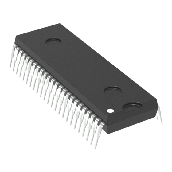
The CY7C130/130A and CY7C140 are available in 48-pin DIP.
The CY7C131/131A and CY7C141 are available in 52-pin
PLCC, 52-pin Pb-free PLCC, 52-pin PQFP, and 52-pin Pb-free
PQFP.
I/O
CONTROL
MEMORY
ADDRESS
ARRAY
DECODER
ARBITRATION
LOGIC
(7C130/7C131 ONLY)
CE
R
AND
INTERRUPT LOGIC
OE
R
R/W
R
•
San Jose
CY7C130, CY7C130A
CY7C131, CY7C131A
CY7C140, CY7C141
[1]
and CY7C141
R/W
R
CE
R
OE
R
I/O
7R
I/O
0R
BUSY
R
A
9R
A
0R
[3]
INT
R
,
CA 95134-1709
•
408-943-2600
Revised December 09, 2008
[+] Feedback
Advertisement
Table of Contents

Related Manuals for Cypress Semiconductor CY7C130


Summary of Contents for Cypress Semiconductor CY7C130
-
Page 1: Functional Description
Logic Block Diagram BUSY Notes 1. CY7C130 and CY7C130A are functionally identical; CY7C131 and CY7C131A are functionally identical. 2. CY7C130/130A/CY7C131/131A (Master): BUSY is open drain output and requires pull-up resistor. CY7C140/CY7C141 (Slave): BUSY is input. 3. Open drain outputs: pull-up resistor required. -
Page 2: Pin Configurations
7C130 7C140 Figure 3. Pin Diagram - PQFP (Top View) 52 5150 49 48 47 1415 16 17 18 19 20 21 22 23 24 25 26 CY7C130, CY7C130A CY7C131, CY7C131A CY7C140, CY7C141 45 44 43 42 41 40 7C131... -
Page 3: Pin Definitions
Data Bus Input/Output Interrupt Flag Busy Flag Power Ground 7C130-30 7C130-35 7C130A-30 7C131-25 7C131-35 7C131-30 7C141-25 7C140-35 7C140-30 7C141-35 7C141-30 CY7C130, CY7C130A CY7C131, CY7C131A CY7C140, CY7C141 Description 7C130-45 7C130-55 7C131-45 7C131-55 7C140-45 7C140-55 7C141-45 7C141-55 Page 3 of 19 Unit [+] Feedback... -
Page 4: Maximum Ratings
Com’l > V – 0.2V, > V – 0.2V < 0.2V, [11] and using AC Test Waveforms input levels of GND to 3V. CY7C130, CY7C130A CY7C131, CY7C131A CY7C140, CY7C141 Ambient Temperature ° ° C to +70 5V ± 10% °... - Page 5 Figure 4. AC Test Loads and Waveforms R1 893Ω OUTPUT 5 pF 347Ω INCLUDING JIGAND SCOPE ALL INPUT PULSES 3.0V 1.40V ≤ 5 ns CY7C130, CY7C130A CY7C131, CY7C131A CY7C140, CY7C141 Unit 281Ω BUSY BUSY Output Load (CY7C130/CY7C131 ONLY) ≤5ns Page 5 of 19 [+] Feedback...
-
Page 6: Switching Characteristics
[10] is less than t and t HZCE LZCE HZOE = 5 pF as in part (b) of AC Test Loads. Transition is measured ±500 mV from steady state voltage. CY7C130, CY7C130A CY7C131, CY7C131A CY7C140, CY7C141 7C130-30 7C130-25 7C130A-30 7C131-25... - Page 7 R/W for Port B is toggled during valid read. Document #: 38-06002 Rev. *E [7, 12] (continued) 7C131-15 7C131A-15 7C141-15 [17] [17] Note 19 Note 19 [17] [17] [17] CY7C130, CY7C130A CY7C131, CY7C131A CY7C140, CY7C141 7C130-30 7C130-25 7C130A-30 7C131-25 7C131-30 7C140-25 Unit 7C140-30 7C141-25 7C141-30 Note 19...
- Page 8 Document #: 38-06002 Rev. *E [7,12] 7C130-35 7C131-35 7C140-35 7C141-35 [10] [17] [17] Note 19 Note 19 [17] [17] [17] CY7C130, CY7C130A CY7C131, CY7C131A CY7C140, CY7C141 7C130-45 7C130-55 7C131-45 7C131-55 7C140-45 7C140-55 Unit 7C141-45 7C141-55 Note 19 Note 19 Note 19...
-
Page 9: Switching Waveforms
Switching Waveforms ADDRESS DATA OUT PREVIOUS DATA VALID LZOE LZCE DATA OUT Read with BUSY, Master: CY7C130 and CY7C131 ADDRESS ADDRESS BUSY DOUT Notes 20. R/W is HIGH for read cycle. 21. Device is continuously selected, CE = V and OE = V 22. - Page 10 Either Port DATA VALID HIGH IMPEDANCE DATA VALID HZWE HIGH IMPEDANCE or t HZWE CY7C130, CY7C130A CY7C131, CY7C131A CY7C140, CY7C141 [16, 23] [17, 24] LZWE to allow the data I/O pins to enter high impedance Page 10 of 19 [+] Feedback...
- Page 11 ADDRESS BUSY Right Address Valid First: ADDRESS MATCH ADDRESS ADDRESS BUSY Document #: 38-06002 Rev. *E ADDRESS MATCH ADDRESS MATCH or t ADDRESS MISMATCH or t ADDRESS MISMATCH CY7C130, CY7C130A CY7C131, CY7C131A CY7C140, CY7C141 Page 11 of 19 [+] Feedback...
- Page 12 Switching Waveforms (continued) Write with BUSY (Slave:CY7C140/CY7C141) BUSY Document #: 38-06002 Rev. *E Figure 12. Busy Timing Diagram No. 3 CY7C130, CY7C130A CY7C131, CY7C131A CY7C140, CY7C141 Page 12 of 19 [+] Feedback...
- Page 13 Left Side Clears INT ADDR Document #: 38-06002 Rev. *E Figure 13. Interrupt Timing Diagrams WRITE 3FF EINS WINS EINR OINR EINS WINS EINR CY7C130, CY7C130A CY7C131, CY7C131A CY7C140, CY7C141 READ 3FF READ 3FE OINR Page 13 of 19 [+] Feedback...
- Page 14 30.0 25.0 20.0 15.0 10.0 = 4.5V = 4.5V = 25°C 1000 CAPACITANCE (pF) CY7C130, CY7C130A CY7C131, CY7C131A CY7C140, CY7C141 OUTPUT SOURCE CURRENT vs. OUTPUT VOLTAGE = 5.0V = 25°C OUTPUT VOLTAGE (V) OUTPUT SINK CURRENT vs. OUTPUT VOLTAGE = 5.0V = 25°C...
-
Page 15: Ordering Information
52-Pin Plastic Leaded Chip Carrier 52-Pin Pb-Free Plastic Leaded Chip Carrier 52-Pin Plastic Quad Flatpack 52-Pin Pb-Free Plastic Quad Flatpack 48-Pin (600 Mil) Molded DIP 48-Pin (600 Mil) Molded DIP CY7C130, CY7C130A CY7C131, CY7C131A CY7C140, CY7C141 Operating Range Commercial Industrial... - Page 16 52-Pin Plastic Quad Flatpack 52-Pin Plastic Leaded Chip Carrier 52-Pin Plastic Quad Flatpack 52-Pin Plastic Leaded Chip Carrier 52-Pin Plastic Quad Flatpack 52-Pin Plastic Leaded Chip Carrier 52-Pin Plastic Quad Flatpack CY7C130, CY7C130A CY7C131, CY7C131A CY7C140, CY7C141 Operating Range Commercial Industrial...
-
Page 17: Package Diagrams
Figure 14. 48-Pin (600 Mil) Sidebraze DIP D26 MIL-STD-1835 D-14 Config. C SEATING PLANE 0.045 0.055 0.023 0.033 0.750 0.756 0.785 0.795 CY7C130, CY7C130A CY7C131, CY7C131A CY7C140, CY7C141 51-80044 ** MIN. DIMENSIONS IN INCHES MAX. 0.013 0.021 0.690 0.730 0.020 MIN. - Page 18 Package Diagrams (continued) Figure 17. 52-Pin Pb-Free Plastic Quad Flatpack N52 Document #: 38-06002 Rev. *E Figure 16. 48-Pin (600 Mil) Molded DIP P25 CY7C130, CY7C130A CY7C131, CY7C131A CY7C140, CY7C141 51-85020-*B 51-85042-** Page 18 of 19 [+] Feedback...
- Page 19 Document History Page Document Title: CY7C130/CY7C130A/CY7C131/CY7C131A/CY7C140/CY7C141 1K x 8 Dual-Port Static RAM Document Number: 38-06002 Orig. of Rev. ECN No. Change 110169 122255 236751 325936 393153 2623540 VKN/PYRS Sales, Solutions, and Legal Information Worldwide Sales and Design Support Cypress maintains a worldwide network of offices, solution centers, manufacturer’s representatives, and distributors. To find the office closest to you, visit us at cypress.com/sales.
Need help?
Do you have a question about the CY7C130 and is the answer not in the manual?
Questions and answers