Table of Contents
Advertisement
Quick Links
Features
■
True dual-ported memory cells that enable simultaneous reads
of the same memory location
■
2K x 8 organization
■
0.65 micron CMOS for optimum speed and power
■
High speed access: 15 ns
■
Low operating power: I
= 110 mA (maximum)
CC
■
Fully asynchronous operation
■
Automatic power down
■
Master CY7C132/CY7C136/CY7C136A
bus width to 16 or more bits using slave CY7C142/CY7C146
■
BUSY output flag on CY7C132/CY7C136/CY7C136A;
BUSY input on CY7C142/CY7C146
■
INT flag for port to port communication (52-Pin PLCC/PQFP
versions)
■
CY7C136, CY7C136A, and CY7C146 available in 52-pin
PLCC and 52-pin PQFP packages
■
Pb-free packages available
Logic Block Diagram
R/W
L
CE
L
OE
L
I/O
7L
I/O
0L
[2]
BUSY
L
A
10L
A
0L
[3]
INT
L
Notes
1. CY7C136 and CY7C136A are functionally identical.
2. CY7C132/CY7C136/CY7C136A (Master): BUSY is open drain output and requires pull up resistor. CY7C142/CY7C146 (Slave): BUSY is input.
3. Open drain outputs; pull up resistor required.
Cypress Semiconductor Corporation
Document #: 38-06031 Rev. *E
Functional Description
The CY7C132, CY7C136, CY7C136A, CY7C142, and CY7C146
are high speed CMOS 2K x 8 dual-port static RAMs. Two ports
are provided to permit independent access to any location in
memory. The CY7C132, CY7C136, and CY7C136A can be used
as either a standalone 8-bit dual-port static RAM or as a
MASTER
CY7C142/CY7C146 SLAVE dual-port device. They are used in
systems that require 16-bit or greater word widths. This is the
solution to applications that require shared or buffered data, such
as cache memory for DSP, bit-slice, or multiprocessor designs.
Each port has independent control pins; chip enable (CE), write
enable (R/W), and output enable (OE). BUSY flags are provided
[1]
easily expands data
on each port. In addition, an interrupt flag (INT) is provided on
each port of the 52-pin PLCC version. BUSY signals that the port
is trying to access the same location currently being accessed
by the other port. On the PLCC version, INT is an interrupt flag
indicating that data is placed in an unique location (7FF for the
left port and 7FE for the right port).
An automatic power down feature is controlled independently on
each port by the chip enable (CE) pins.
I/O
CONTROL
MEMORY
ADDRESS
ARRAY
DECODER
ARBITRATION
LOGIC
(7C132/7C136 ONLY)
AND
CE
L
INTERRUPTLOGIC
(7C136/7C146 ONLY)
OE
L
R/W
L
•
198 Champion Court
CY7C132, CY7C136
CY7C136A, CY7C142, CY7C146
2K x 8 Dual-Port Static RAM
dual-port
RAM,
in
R/W
CE
OE
I/O
I/O
CONTROL
I/O
BUSY
A
10R
ADDRESS
DECODER
A
0R
CE
R
OE
R
R/W
R
INT
,
•
San Jose
CA 95134-1709
conjunction
with
the
R
R
R
7R
0R
[2]
R
[3]
R
•
408-943-2600
Revised March 24, 2009
[+] Feedback
Advertisement
Table of Contents

Related Manuals for Cypress Semiconductor Perform CY7C132


Summary of Contents for Cypress Semiconductor Perform CY7C132
-
Page 1: Functional Description
Features ■ True dual-ported memory cells that enable simultaneous reads of the same memory location ■ 2K x 8 organization ■ 0.65 micron CMOS for optimum speed and power ■ High speed access: 15 ns ■ Low operating power: I = 110 mA (maximum) ■... -
Page 2: Selection Guide
Pinouts Figure 1. 52-Pin PLCC (Top View) 7 6 5 4 3 2 52 51 50 49 48 47 7C136/7C136A 7C146 2122 23 24 25 26 27 28 29 30 31 32 33 Selection Guide Specification Maximum Access Time Maximum Operating Current Com’l/Ind Maximum Standby Current Com’l/Ind Shaded areas contain preliminary information. -
Page 3: Maximum Ratings
Maximum Ratings Exceeding maximum ratings may impair the useful life of the device. These user guidelines are not tested. Storage Temperature ... −65°C to +150°C Ambient Temperature with Power Applied... −55°C to +125°C Supply Voltage to Ground Potential (Pin 48 to Pin 24)...−0.5V to +7.0V DC Voltage Applied to Outputs in High Z State ...−0.5V to +7.0V Electrical Characteristics... -
Page 4: Switching Characteristics
Capacitance This parameter is guaranteed but not tested. Parameter Description Input Capacitance Output Capacitance R1 893Ω OUTPUT 30 pF 347Ω INCLUDING JIG AND SCOPE Equivalent to: TH ÉVENIN EQUIVALENT 250Ω OUTPUT Switching Characteristics Over the Operating Range (Speeds -15, -25, -30) Parameter Description Read Cycle... - Page 5 Switching Characteristics Over the Operating Range (Speeds -15, -25, -30) Parameter Description [12] Write Cycle Write Cycle Time CE LOW to Write End Address Setup to Write End Address Hold from Write End Address Setup to Write Start R/W Pulse Width Data Setup to Write End Data Hold from Write End R/W LOW to High Z...
- Page 6 Switching Characteristics Over the Operating Range (Speeds -35, -45, -55) Parameter Description Read Cycle Read Cycle Time Address to Data Valid Data Hold from Address Change CE LOW to Data Valid OE LOW to Data Valid [7, 10] OE LOW to Low Z LZOE [7, 10, 11] OE HIGH to High Z...
-
Page 7: Switching Waveforms
Switching Characteristics Over the Operating Range (Speeds -35, -45, -55) Parameter Description [16] Interrupt Timing R/W to INTERRUPT Set Time WINS CE to INTERRUPT Set Time EINS Address to INTERRUPT Set Time OE to INTERRUPT Reset Time OINR CE to INTERRUPT Reset Time EINR Address to INTERRUPT Reset Time Switching Waveforms... - Page 8 Switching Waveforms (continued) Figure 6. Read Cycle No. 3 (Read with BUSY Master: CY7C132 and CY7C136/CY7C136A) ADDRESS ADDRESS BUSY DOUT Figure 7. Write Cycle No.1 (OE Three-States Data I/Os—Either Port) ADDRESS DATA HZOE Note 20. If OE is LOW during a R/W controlled write cycle, the write pulse width must be the larger of t and for data to be placed on the bus for the required t Document #: 38-06031 Rev.
- Page 9 Switching Waveforms (continued) Figure 8. Write Cycle No. 2 (R/W Three-States Data I/Os—Either Port) ADDRESS DATA Figure 9. Busy Timing Diagram No. 1 (CE Arbitration) Valid First: ADDRESS BUSY Valid First: ADDRESS BUSY Note 21. If the CE LOW transition occurs simultaneously with or after the R/W LOW transition, the outputs remain in a high impedance state. Document #: 38-06031 Rev.
- Page 10 Switching Waveforms (continued) Figure 10. Busy Timing Diagram No. 2 (Address Arbitration) Left Address Valid First: ADDRESS ADDRESS MATCH ADDRESS BUSY Right Address Valid First: ADDRESS ADDRESS MATCH ADDRESS BUSY Figure 11. Busy Timing Diagram No. 3 (Write with BUSY, Slave: CY7C142/CY7C146) BUSY Document #: 38-06031 Rev.
- Page 11 Switching Waveforms (continued) [16] Interrupt Timing Diagrams ADDRESS R/ W ADDRESS ADDRESS ADDRESS R/ W Document #: 38-06031 Rev. *E CY7C136A, CY7C142, CY7C146 Figure 12. Left Side Sets INT WRITE 7FF EINS WINS Figure 13. Right Side Clears INT EINR Figure 14.
- Page 12 NORMALIZED SUPPLY CURRENT vs. SUPPLY VOLTAGE SUPPLY VOLTAGE (V) NORMALIZED ACCESS TIME vs. SUPPLY VOLTAGE = 25°C SUPPLY VOLTAGE (V) TYPICAL POWER-ON CURRENT vs. SUPPLY VOLTAGE SUPPLY VOLTAGE (V) Document #: 38-06031 Rev. *E CY7C136A, CY7C142, CY7C146 Figure 16. Typical DC and AC Characteristics NORMALIZED SUPPLY CURRENT vs.
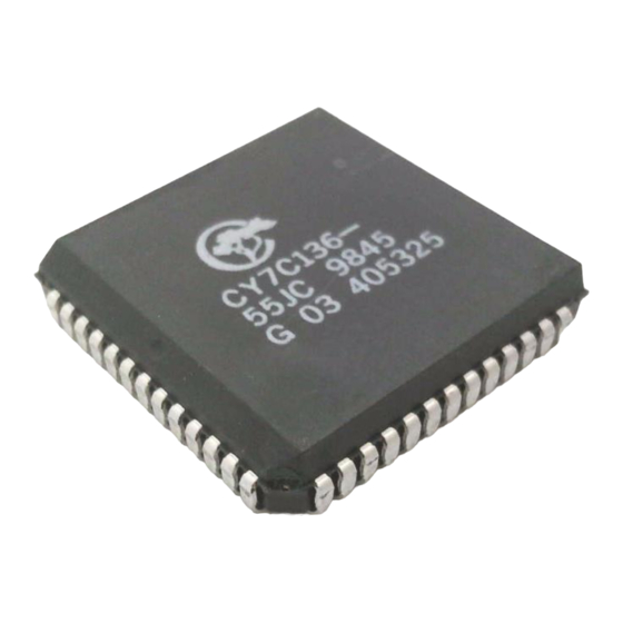
- Page 13 Ordering Information Speed Ordering Code (ns) CY7C136-15JC CY7C136-15NC CY7C136-25JC CY7C136-25JXC CY7C136-25NC CY7C136-25NXC CY7C136-25JXI CY7C136-30JC CY7C136-30NC CY7C136-30JI CY7C136-35JC CY7C136-35NC CY7C136-35JI CY7C136-45JC CY7C136-45NC CY7C136-45JI CY7C136-55JC CY7C136-55JXC CY7C136-55NC CY7C136-55NXC CY7C136-55JI CY7C136A-55JXI CY7C136-55NI CY7C136A-55NXI CY7C146-15JC CY7C146-15NC CY7C146-25JC CY7C146-25JXC CY7C146-25NC CY7C146-30JC CY7C146-30NC CY7C146-30JI CY7C146-35JC CY7C146-35NC CY7C146-35JI CY7C146-45JC CY7C146-45NC...
-
Page 14: Package Diagrams
CY7C132, CY7C136 CY7C136A, CY7C142, CY7C146 Package Diagrams Figure 17. 52-Pin Plastic Leaded Chip Carrier, 51-85004 51-85004-*A Figure 18. 52-Pin Plastic Quad Flatpack, 51-85042 51-85042-** Document #: 38-06031 Rev. *E Page 14 of 15 [+] Feedback... - Page 15 Document History Page Document Title: CY7C132, CY7C136, CY7C136A, CY7C142, CY7C146 2K x 8 Dual-Port Static RAM Document Number: 38-06031 Submission Orig. of Revision Date Change 110171 10/21/01 128959 09/03/03 236748 See ECN 393184 See ECN 2623658 12/17/08 VKN/PYRS Added CY7C136-25JXI part 2678221 03/24/2009 VKN/AESA Added CY7C136A-55JXI, and CY7C136A-55NXI parts.
Need help?
Do you have a question about the Perform CY7C132 and is the answer not in the manual?
Questions and answers