Table of Contents
Advertisement
Quick Links
Features
■
20 ns, 25 ns, and 45 ns access times
■
Internally organized as 1024K x 8 (CY14B108K) or 512K x 16
(CY14B108M)
■
Hands off automatic STORE on power down with only a small
capacitor
®
■
STORE to QuantumTrap
nonvolatile elements is initiated by
software, device pin, or AutoStore
■
RECALL to SRAM initiated by software or power up
■
High reliability
■
Infinite Read, Write, and RECALL cycles
■
200,000 STORE cycles to QuantumTrap
■
20 year data retention
■
Single 3V +20%, –10% operation
■
Data integrity of Cypress nvSRAM combined with full featured
Real Time Clock (RTC)
Logic Block Diagram
A
0
A
1
A
2
A
3
A
4
A
5
A
6
A
7
A
8
A
17
A
18
A
19
DQ
0
DQ
1
DQ
2
DQ
3
DQ
4
DQ
5
DQ
6
DQ
7
DQ
8
DQ
9
DQ
10
DQ
11
DQ
12
DQ
13
DQ
14
DQ
15
Notes
1. Address A
- A
for x8 configuration and Address A
0
19
2. Data DQ
- DQ
for x8 configuration and Data DQ
0
7
3. BHE and BLE are applicable for x16 configuration only.
Cypress Semiconductor Corporation
Document #: 001-47378 Rev. **
PRELIMINARY
8 Mbit (1024K x 8/512K x 16) nvSRAM with
®
on power down
[1, 2, 3]
R
O
W
D
E
STATIC RAM
C
ARRAY
O
2048 X 2048 X 2
D
E
R
I
N
P
U
T
B
COLUMN I/O
U
F
F
E
R
COLUMN DEC
S
A
A
A
A
A
A
9
10
11
12
13
14
- A
for x16 configuration.
0
18
- DQ
for x16 configuration.
0
15
•
198 Champion Court
CY14B108K, CY14B108M
■
Watchdog timer
■
Clock alarm with programmable interrupts
■
Capacitor or battery backup for RTC
■
Commercial and industrial temperatures
■
44 and 54-pin TSOP II package
■
Pb-free and RoHS compliance
Functional Description
The Cypress CY14B108K/CY14B108M combines a 8-Mbit
nonvolatile static RAM with a full featured RTC in a monolithic
integrated circuit. The embedded nonvolatile elements incor-
porate QuantumTrap technology producing the world's most
reliable nonvolatile memory. The SRAM is read and written
infinite number of times, while independent nonvolatile data
resides in the nonvolatile elements.
The RTC function provides an accurate clock with leap year
tracking and a programmable, high accuracy oscillator. The
alarm function is programmable for periodic minutes, hours,
days, or months alarms. There is also a programmable watchdog
timer for process control.
V
Quatrum
V
CAP
CC
Trap
2048 X 2048 X 2
POWER
CONTROL
STORE
RECALL
STORE/RECALL
CONTROL
SOFTWARE
DETECT
A
A
15
16
•
San Jose
Real Time Clock
V
RTCbat
V
RTCcap
HSB
A
- A
14
2
X
out
RTC
X
in
INT
MUX
A
- A
19
0
OE
WE
CE
BLE
BHE
,
CA 95134-1709
•
408-943-2600
Revised April 01, 2009
[+] Feedback
Advertisement
Table of Contents

Related Manuals for Cypress CY14B108K


Summary of Contents for Cypress CY14B108K
-
Page 1: Real Time Clock
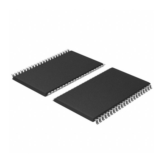
Features ■ 20 ns, 25 ns, and 45 ns access times ■ Internally organized as 1024K x 8 (CY14B108K) or 512K x 16 (CY14B108M) ■ Hands off automatic STORE on power down with only a small capacitor ® ■ STORE to QuantumTrap nonvolatile elements is initiated by ®... - Page 2 4. Address expansion for 16 Mbit. NC pin not connected to die. Document #: 001-47378 Rev. ** PRELIMINARY RTCcap Xout RTCbat Description - DQ - DQ CY14B108K, CY14B108M 54 - TSOP II (x16) Top View (not to scale) RTCcap RTCbat is used. RTCbat is used.
-
Page 3: Device Operation
Power Supply AutoStore Capacitor. Supplies power to the nvSRAM during power loss to store data from SRAM to nonvolatile elements. Device Operation The CY14B108K/CY14B108M nvSRAM is made up of two functional components paired in the same physical cell. These are a SRAM memory cell and a nonvolatile QuantumTrap cell. - Page 4 HSB signal is monitored by the system to detect if an AutoStore cycle is in progress. Hardware STORE (HSB) Operation The CY14B108K/CY14B108M provides the HSB pin to control and acknowledge the STORE operations. The HSB pin is used to request a Hardware STORE cycle. When the HSB pin is driven...
- Page 5 A sequence of read operations is performed in a Notes 5. While there are 20 address lines on the CY14B108K (19 address lines on the CY14B108M), only the 13 address lines (A The remaining address lines are don’t care.
-
Page 6: Data Protection
CY14B108K/CY14B108M is in a write mode (both CE and WE are LOW) at power up, after a RECALL or STORE, the write is inhibited until the SRAM is enabled after t active). This protects against inadvertent writes during power up or brown out conditions. -
Page 7: Real Time Clock Operation
Double buffering also circumvents disrupting normal timing counts or the clock accuracy of the internal clock when accessing clock data. Clock and alarm registers store data in BCD format. RTC functionality is described with respect to CY14B108K in the following sections. same description CY14B108M, except for the RTC register addresses. -
Page 8: Watchdog Timer
‘W’ bit back to “0” for the changes to take effect. Note CY14B108K requires the alarm match bit for seconds (0xFFFF2 - D7) to be set to ‘0’ for proper operation of Alarm Flag and Interrupt. -
Page 9: Power Monitor
Watchdog Register Power Monitor The CY14B108K provides a power management scheme with power fail interrupt capability. It also controls the internal switch to backup power for the clock and protects the memory from low access. The power monitor is based on an internal band gap reference circuit that compares the V threshold. - Page 10 = 21 pF Note: The recommended values for C1 and C2 include board trace capacitance. Figure 5. Interrupt Block Diagram Driver CY14B108K, CY14B108M WDF - Watchdog Timer Flag WIE - Watchdog Interrupt Enable PF - Power Fail Flag PFE - Power Fail Enable...
- Page 11 Table 4. RTC Register Map Register CY14B108K CY14B108M 0xFFFFF 0x7FFFF 0xFFFFE 0x7FFFE 0xFFFFD 0x7FFFD 0xFFFFC 0x7FFFC 0xFFFFB 0x7FFFB 0xFFFFA 0x7FFFA 0xFFFF9 0x7FFF9 0xFFFF8 0x7FFF8 OSCEN 0xFFFF7 0x7FFF7 0xFFFF6 0x7FFF6 WIE (0) 0xFFFF5 0x7FFF5 M (1) 0xFFFF4 0x7FFF4 M (1) 0xFFFF3...
- Page 12 10s Day of Month Time Keeping - Day Time Keeping - Hours 10s Hours Time Keeping - Minutes 10s Minutes Time Keeping - Seconds 10s Seconds CY14B108K, CY14B108M Years Months Day of Month Day of Week Hours Minutes Seconds Page 12 of 29...
- Page 13 Document #: 001-47378 Rev. ** PRELIMINARY Description Calibration/Control Calibration Sign WatchDog Timer Interrupt Status/Control Alarm - Day 10s Alarm Date CY14B108K, CY14B108M Calibration Watchdog Timer on page 8. Alarm Date Page 13 of 29 [+] Feedback...
- Page 14 10s Alarm Seconds Time Keeping - Centuries 10s Centuries Flags OSCF . It is cleared to 0 when the Flags register is read or on power up. CY14B108K, CY14B108M Alarm Hours Alarm Minutes Alarm Seconds Centuries Page 14 of 29...
-
Page 15: Maximum Ratings
= –2 mA = 4 mA pin and V , 5V Rated DC Electrical Characteristics are average values at 25°C (room temperature), and V CY14B108K, CY14B108M + 2.0V = 25°C) ... 1.0W Ambient Temperature 0°C to +70°C 2.7V to 3.6V –40°C to +85°C... -
Page 16: Ac Test Conditions
Test conditions follow standard test methods and procedures for measuring thermal impedance, in accordance with EIA/JESD51. Figure 6. AC Test Loads 577Ω 3.0V OUTPUT 789Ω CY14B108K, CY14B108M Unit Years Unit 44 TSOP II 54 TSOP II Unit °C/W 31.11 30.73 °C/W... - Page 17 RTC Capacitor Pin Voltage RTCcap tOCS RTC Oscillator Time to Start Note 14. From either V or V RTCcap RTCbat. Document #: 001-47378 Rev. ** PRELIMINARY Test Conditions Room Temperature (25 Hot Temperature (85 CY14B108K, CY14B108M Units Page 17 of 29 [+] Feedback...
-
Page 18: Switching Waveforms
19. HSB must remain HIGH during Read and Write cycles. Document #: 001-47378 Rev. ** PRELIMINARY 20 ns Description [15, 16, 19] Address Valid CY14B108K, CY14B108M 25 ns 45 ns Unit Output Data Valid Page 18 of 29 [+] Feedback... - Page 19 Document #: 001-47378 Rev. ** PRELIMINARY [3, 15, 19] Address Valid LZCE LZOE LZBE Output Data Valid Active [3, 18, 19, 20] Address Valid Input Data Valid LZWE HZWE High Impedance CY14B108K, CY14B108M HZCE HZOE HZBE Page 19 of 29 [+] Feedback...
- Page 20 21. Only CE and WE controlled writes to RTC registers are allowed. BLE pin must be held LOW before CE or WE pin goes LOW for writes to RTC register. Document #: 001-47378 Rev. ** PRELIMINARY [3, 18, 19, 20] Address Valid Input Data Valid High Impedance Address Valid Input Data Valid High Impedance CY14B108K, CY14B108M [5, 18, 19, 20, 21] Page 20 of 29 [+] Feedback...
- Page 21 STORE HHHD LZHSB DELAY HRECALL Read & Write BROWN POWER-UP RECALL Autostore SWITCH. SWITCH. Ω resistor, HSB driver is disabled. CY14B108K, CY14B108M 25 ns 45 ns 2.65 2.65 [25] Note STORE Note HHHD DELAY LZHSB HRECALL Read & Write POWER...
- Page 22 Address #6 DELAY HZCE Figure 14. AutoStore Enable and Disable Cycle Address #6 HZCE DELAY Table 2. WE must be HIGH during all six consecutive cycles. CY14B108K, CY14B108M [27, 28] 25 ns 45 ns [28] HHHD LZHSB High Impedance STORE...
- Page 23 SRAM is disabled as long as HSB (IN) is driven low. DHSB DHSB [31, 32] Figure 16. Soft Sequence Processing Soft Sequence Command Address #6 Address #1 CY14B108K, CY14B108M 25 ns 45 ns Unit HHHD LZHSB only by Internal Address #6 Page 23 of 29...
- Page 24 High-Z Output Disabled Data In (DQ –DQ Write Data In (DQ –DQ Write –DQ in High-Z Data In (DQ –DQ Write –DQ in High-Z CY14B108K, CY14B108M Mode Power Standby Active Active Active Mode Power Standby Active Active Active Active Active...
-
Page 25: Part Numbering Nomenclature
C - Commercial (0 to 70°C) I - Industrial (–40 to 85°C) Pb-Free Package: ZS - TSOP II Voltage: B - 3.0V CY14B108K, CY14B108M Speed: 20 - 20 ns 25 - 25 ns 45 - 45 ns Data Bus: K - x8 + RTC... -
Page 26: Ordering Information
44-pin TSOPII 51-85087 44-pin TSOPII 51-85087 44-pin TSOPII 51-85187 44-pin TSOPII 51-85160 54-pin TSOPII 51-85160 54-pin TSOPII 51-85160 54-pin TSOPII 51-85160 54-pin TSOPII CY14B108K, CY14B108M Operating Range Commercial Industrial Commercial Industrial Commercial Industrial Commercial Industrial Commercial Industrial Commercial Industrial Page 26 of 29... -
Page 27: Package Diagrams
Figure 17. 44-Pin TSOP II (51-85087) PIN 1 I.D. BASE PLANE 0°-5° 0.10 (.004) 0.597 (0.0235) 0.406 (0.0160) SEATING PLANE CY14B108K, CY14B108M DIMENSION IN MM (INCH) MIN. EJECTOR PIN BOTTOM VIEW 10.262 (0.404) 10.058 (0.396) 0.210 (0.0083) 0.120 (0.0047) 51-85087 *A... - Page 28 PRELIMINARY CY14B108K, CY14B108M Package Diagrams (continued) Figure 18. 54-Pin TSOP II (51-85160) 51-85160 ** Document #: 001-47378 Rev. ** Page 28 of 29 [+] Feedback...
- Page 29 Document History Page Document Title: CY14B108K/CY14B108M 8 Mbit (1024K x 8/512K x 16) nvSRAM with Real Time Clock Document Number: 001-47378 Orig. of Submission Rev. ECN No. Change Date 2681767 GVCH/PYRS 04/01/09 Sales, Solutions, and Legal Information Worldwide Sales and Design Support Cypress maintains a worldwide network of offices, solution centers, manufacturer’s representatives, and distributors.
Need help?
Do you have a question about the CY14B108K and is the answer not in the manual?
Questions and answers