Table of Contents
Advertisement
Quick Links
Features
®
■
Meets Rambus
Extended Data Rate (XDR™) clocking
requirements
■
25 ps typical cycle-to-cycle jitter
❐
–135 dBc/Hz typical phase noise at 20 MHz offset
■
100 or 133 MHz differential clock input
■
300–667 MHz high speed clock support
■
Quad (open drain) differential output drivers
■
Supports frequency multipliers: 3, 4, 5, 6, 9/2 and 15/4
■
Spread Aware™
■
2.5V operation
■
28-pin TSSOP package
Logic Block Diagram
REFCLK,REFCLKB
Cypress Semiconductor Corporation
Document Number: 001-42414 Rev. **
®
Rambus
/BYPASS
EN
RegA
RegB
Bypass
MUX
RegC
PLL
RegD
SCL
SDA
ID0
ID1
•
198 Champion Court
XDR™ Clock Generator with
Zero SDA Hold Time
Table 1. Device Comparison
CY24271
SDA hold time = 300 ns
(SMBus compliant)
R
= 200Ω typical
RC
(Rambus standard drive)
EN
EN
EN
EN
,
•
San Jose
CA 95134-1709
CY24272
CY24272
SDA hold time = 0 ns
2
(I
C compliant)
R
= 295Ω minimum
RC
(Reduced output drive)
CLK0
CLK0B
CLK1
CLK1B
CLK2
CLK2B
CLK3
CLK3B
•
408-943-2600
Revised November 9, 2007
[+] Feedback
Advertisement
Table of Contents

Related Manuals for Cypress Semiconductor Rambus XDR CY24271


Summary of Contents for Cypress Semiconductor Rambus XDR CY24271
- Page 1 ■ 25 ps typical cycle-to-cycle jitter ❐ –135 dBc/Hz typical phase noise at 20 MHz offset ■ 100 or 133 MHz differential clock input ■ 300–667 MHz high speed clock support ■ Quad (open drain) differential output drivers ■...
- Page 2 2.5V power supply for phased lock loop (PLL) Ground Set clock driver current (external resistor) Ground Reference clock input (connect to clock source) Complement of reference clock (connect to clock source) 2.5V power supply for core Ground SMBus clock (connect to SMBus) SMBus data (connect to SMBus)
- Page 3 100 MHz and 133.3 MHz. The PLL multipliers are applicable to spread spectrum modulated input clock with maximum and minimum input cycle time. The REFSEL bit in SMBus 81h is set correctly as shown.
- Page 4 CLK/CLKB CLK/CLKB SMBus Data Byte Definitions Three data bytes are defined for the CY24272. Byte 0 is for programming the PLL multiplier registers and clock output registers. The definition of Byte 2 is shown in on page 5. The upper five bits are the revision numbers of the device and the lower three bits are the ID numbers assigned to the vendor by Rambus.
- Page 5 Rambus assigned Vendor ID Code Table 3 on page 3 for PLL multipliers and CY24272 Table 3 on page 3) Table 3 on page 3) Table 5 on page 4 for clock output selections. Page 5 of 13 [+] Feedback...
-
Page 6: Differential Input
Figure 2. Differential and Single-Ended Clock Inputs REFCLKB Input REFCLK XDR Clock Generator Differential Input Absolute Maximum Conditions Parameter Description Clock Buffer Supply Voltage Core Supply Voltage PLL Supply Voltage Input Voltage (SCL and SDA) Input Voltage (REFCLK/REFCLKB Input Voltage... -
Page 7: Dc Operating Conditions
DC Operating Conditions Parameter Description Supply Voltage for PLL Supply Voltage for Core Supply Voltage for Clock Buffers Input High Voltage, REFCLK/REFCLKB IHCLK Input Low Voltage, REFCLK/REFCLKB ILCLK Crossing Point Voltage, REFCLK/REFCLKB IXCLK ΔV Difference in Crossing Point Voltage, REFCLK/REFCLKB... -
Page 8: Dc Electrical Specifications
0.6% triangular modulation. Typically, the amount of allowed non-triangular modulation is about 0.5%. 13. V is measured on external divider network. 14. V = (clock output high voltage – clock output low voltage), measured on the external divider network. 15. V is measured at the clock output pins of the package. OL_ABS 16. - Page 9 Parameter [19] Clock Cycle time CYCLE Jitter over 1-6 clock cycles at 400–635 MHz JIT(cc) Jitter over 1-6 clock cycles at 638–667 MHz Phase noise SSB spectral purity L(f) at 20 MHz offset: 400–500 MHz (In addition, device must not exceed L(f) = 10log[1+(50x10 f = 1 MHz to 100 MHz except for the region near f = REFCLK/Q where Q is the value of the internal reference divider.)
-
Page 10: Signal Waveforms
–V Notes 19. Max and min output clock cycle times are based on nominal outputs frequency of 300 and 667 MHz, respectively. For spread spectrum modulated differential or single-ended REFCLK, the output clock tracks the modulation of the input. 20. Output short term jitter spec is the absolute value of the worst case deviation. - Page 11 CLKB CLKB CYCLE,i CLKB DC,ERR Document Number: 001-42414 Rev. ** Figure 4. Input and Output Waveforms Figure 5. Crossing Point Voltage Figure 6. Cycle-to-cycle Jitter CYCLE,i+1 CYCLE,i CYCLE,i+1 over 10,000 consecutive cycles Figure 7. Cycle-to-cycle Duty-cycle Error (i+1) (i+1) CYCLE, CYCLE, (i) - t (i+1) and t...
-
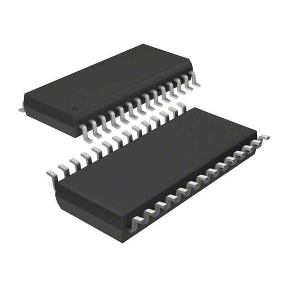
Page 12: Ordering Information
Ordering Information Part Number Pb-Free CY24272ZXC CY24272ZXCT Package Drawing and Dimension Figure 8. 28-Pin Thin Shrunk Small Outline Package (4.40-mm Body) ZZ28 0.65[0.025] BSC. 0.85[0.033] 0.95[0.037] 9.60[0.378] 9.80[0.386] Document Number: 001-42414 Rev. ** Package Type 28-pin TSSOP 28-pin TSSOP – Tape and Reel PIN 1 ID 6.25[0.246] 6.50[0.256]... - Page 13 Document History Page ® Document Title: CY24272 Rambus XDR™ Clock Generator with Zero SDA Hold Time Document Number: 001-42414 Issue Orig. of REV. ECN NO. Date Change 1749003 See ECN KVM/AESA New data sheet © Cypress Semiconductor Corporation, 2007. The information contained herein is subject to change without notice. Cypress Semiconductor Corporation assumes no responsibility for the use of any circuitry other than circuitry embodied in a Cypress product.
Need help?
Do you have a question about the Rambus XDR CY24271 and is the answer not in the manual?
Questions and answers