Table of Contents
Advertisement
Quick Links
Features
■
All output pair skew <100 ps typical (250 max)
■
3.75 to 110 MHz output operation
■
User selectable output functions
❐
Selectable skew to 18 ns
❐
Inverted and non-inverted
1
⁄
1
⁄
❐
Operation at
and
2
4
❐
Operation at 2x and 4x input frequency (input as low as
3.75 MHz)
■
Zero input-to-output delay
■
50% duty cycle outputs
■
LVTTL outputs drive 50Ω terminated lines
■
Operates from a single 3.3V supply
■
Low operating current
■
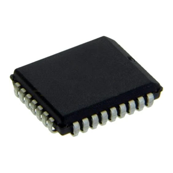
32-pin PLCC package
■
Jitter 100 ps (typical)
Logic Block Diagram
Cypress Semiconductor Corporation
Document Number: 38-07408 Rev. *D
High Speed Low Voltage Programmable Skew
input frequency
TEST
PHASE
FB
FREQ
FILTER
DET
REF
FS
4F0
4F1
SELECT
INPUTS
(THREE
LEVEL)
3F0
3F1
2F0
2F1
1F0
1F1
•
198 Champion Court
Functional Description
The CY7B9911V 3.3V RoboClock+™ High Speed Low
Voltage Programmable Skew Clock Buffer (LVPSCB) offers
user selectable control over system clock functions. These
multiple output clock drivers provide the system integrator with
functions necessary to optimize the timing of high perfor-
mance computer systems. Each of the eight individual drivers,
arranged in four pairs of user controllable outputs, can drive
terminated transmission lines with impedances as low as 50Ω.
They deliver minimal and specified output skews and full swing logic
levels (LVTTL).
Each output is hardwired to one of nine delay or function
configurations. Delay increments of 0.7 to 1.5 ns are deter-
mined by the operating frequency with outputs that can skew
up to ±6 time units from their nominal "zero" skew position. The
completely integrated PLL allows external load and cancels
the transmission line delay effects. When this "zero delay"
capability of the LVPSCB is combined with the selectable
output skew functions, you can create output-to-output delays
of up to ±12 time units.
Divide-by-two and divide-by-four output functions are provided
for additional flexibility in designing complex clock systems.
When combined with the internal PLL, these divide functions
allow distribution of a low frequency clock that are multiplied
by two or four at the clock destination. This facility minimizes
clock distribution difficulty enabling maximum system clock
speed and flexibility.
VCO AND
TIME UNIT
GENERATOR
4Q0
4Q1
SKEW
3Q0
3Q1
SELECT
2Q0
MATRIX
2Q1
1Q0
1Q1
,
•
San Jose
CA 95134-1709
CY7B9911V
3.3V RoboClock+™
Clock Buffer
•
408-943-2600
Revised June 20, 2007
[+] Feedback
Advertisement
Table of Contents

Related Manuals for Cypress Semiconductor CY7B9911V


Summary of Contents for Cypress Semiconductor CY7B9911V
-
Page 1: Functional Description
Document Number: 38-07408 Rev. *D High Speed Low Voltage Programmable Skew Functional Description The CY7B9911V 3.3V RoboClock+™ High Speed Low Voltage Programmable Skew Clock Buffer (LVPSCB) offers user selectable control over system clock functions. These multiple output clock drivers provide the system integrator with functions necessary to optimize the timing of high perfor- mance computer systems. -
Page 2: Pin Configuration
4Q0, 4Q1 Output pair 4. See Power supply for output drivers. Power supply for internal circuitry. Ground. Document Number: 38-07408 Rev. *D PLCC 32 31 30 CY7B9911V 18 19 20 Description Table “Test Mode” on page 4 under the Table Table... -
Page 3: Block Diagram Description
, LOW indicates a connection to GND, and MID indicates an open connection. Internal termination ) of the V and Time Unit Generator (see). Nominal frequency (f Table /2 or f has reached 2.8V. CY7B9911V 3.3V RoboClock+™ Table 2 shows the nine possible output Output Functions 1Q0, 1Q1,... -
Page 4: Test Mode
Test Mode The TEST input is a three level input. In normal system operation, this pin is connected to ground, allowing the CY7B9911V to operate as described in Description” on page 3. For testing purposes, any of the three level inputs can have a removable jumper to ground or be tied LOW through a 100W resistor. -
Page 5: Operational Mode Descriptions
Figure 2 shows the LVPSCB configured as a zero skew clock buffer. In this mode the CY7B9911V is used as the basis for a low skew clock distribution tree. When all the function select inputs (xF0, xF1) are left open, each of the outputs are aligned and drive a terminated transmission line to an independent load. - Page 6 The divided outputs offer a zero delay divider for portions of the 20 MHz system that divide the clock by either two or four, and still remain within a narrow skew of the “1X” clock. Without this feature, an 80 MHz external divider is added, and the propagation delay of the divider adds to the skew between the different clock signals.
- Page 7 Figure 8 shows the CY7B9911V connected in series to construct a zero skew clock distribution tree between boards. Delays of the downstream clock buffers are programmed to compensate for the wire length (that is, select negative skew equal to the wire delay) necessary to connect them to the master clock source, approximating a zero delay clock tree.
-
Page 8: Maximum Ratings
7. CY7B9911V must be tested one output at a time, output shorted for less than one second, less than 10% duty cycle. Room temperature only. 8. Total output current per output pair is approximated by the following expression that includes device current plus load current: CY7B9911V: ICCN = [(4 + 0.11F) + [[((835 –3F)/Z) + (.0022FC)]N] x 1.1... - Page 9 FS = HIGH [13, 14] [13, 15] [13, 17] [13, 17] [17, 17] [13, 17] [12, 18] [19] [20] [20] [12] [12] Peak-to-Peak CY7B9911V 3.3V RoboClock+™ [10] Unit 3.0V 2.0V =1.5V 0.8V ≤1ns CY7B9911V-5 Unit Table 1 0.25 0.25 1.25 –0.5...
- Page 10 Cycle-to-Cycle Output Jitter Notes 11. Test measurement levels for the CY7B9911V are TTL levels (1.5V to 1.5V). Test conditions assume signal transition times of 2 ns or less and output loading as shown in the AC Test Loads and Waveforms 12.
- Page 11 INVERTED Q REF DIVIDED BY 2 REF DIVIDED BY 4 Document Number: 38-07408 Rev. *D RPWL RPWH ODCV ODCV SKEWPR, SKEWPR, SKEW0,1 SKEW0,1 SKEW2 SKEW3,4 SKEW3,4 SKEW1,3, 4 CY7B9911V 3.3V RoboClock+™ SKEW2 SKEW3,4 SKEW2,4 Page 11 of 14 [+] Feedback...
-
Page 12: Ordering Information
Ordering Information Accuracy (ps) Ordering Code CY7B9911V-5JC CY7B9911V-5JCT [23] CY7B9911V-7JC [23] CY7B9911V-7JCT Pb-Free CY7B9911V-5JXC CY7B9911V-5JXCT [23] CY7B9911V-7JXC [23] CY7B9911V-7JXCT Note 23. Parts not recommended for the new design. Document Number: 38-07408 Rev. *D Package Type 32-Pb Plastic Leaded Chip Carrier 32-Pb Plastic Leaded Chip Carrier –... -
Page 13: Package Diagram
CY7B9911V 3.3V RoboClock+™ Package Diagram Figure 10. 32-Pin Plastic Leaded Chip Carrier J65 51-85002-*B Document Number: 38-07408 Rev. *D Page 13 of 14 [+] Feedback... - Page 14 Document History Page Document Title: CY7B9911V 3.3V RoboClock+™ High Speed Low Voltage Programmable Skew Clock Buffer Document Number: 38-07408 Orig. of REV. ECN NO. Issue Date Change 114350 3/20/02 299713 See ECN 404630 See ECN 1199925 See ECN KVM/AESA Added Note 23: Parts not recommended for the new design in Ordering...
Need help?
Do you have a question about the CY7B9911V and is the answer not in the manual?
Questions and answers