Advertisement
Quick Links
For Quartus II 15.0
1 Introduction
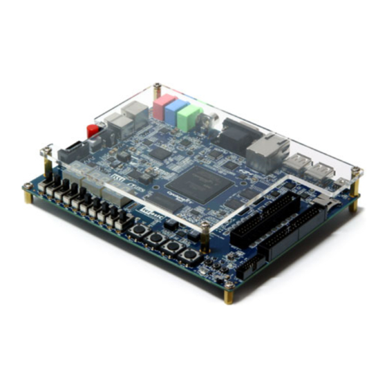
This document describes a computer system that can be implemented on the Altera DE1-SoC development and
education board. This system, called the DE1-SoC Computer, is intended for use in experiments on computer orga-
nization and embedded systems. To support such experiments, the system contains embedded processors, memory,
audio and video devices, and some simple I/O peripherals. The FPGA programming file that implements this system,
as well as its design source files, can be obtained from the University Program section of Altera's web site.
2 DE1-SoC Computer Contents
A block diagram of the DE1-SoC Computer system is shown in Figure 1. As indicated in the figure, the components
in this system are implemented utilizing both the FPGA and the Hard Processor System (HPS) inside Altera's
R
Cyclone
V SoC chip. The FPGA implements two Nios II processors and several peripheral ports: memory, timer
modules, audio-in/out, video-in/out, PS/2, analog-to-digital, infrared receive/transmit, and parallel ports connected
to switches and lights. The HPS comprises an ARM Cortex A9 dual-core processor and a set of peripheral devices.
Instructions for using the HPS and ARM processor are provided in a separate document, called DE1-SoC Computer
System with ARM Cortex-A9.
2.1 FPGA Components
As shown in Figure
1
Cyclone V SoC chip. Several of these components are described in this section, and the others are presented in
Section 4.
2.2 Nios II Processor
R
The Altera Nios
II processor is a 32-bit CPU that can be implemented in an Altera FPGA device. Three versions
of the Nios II processor are available, designated economy (/e), standard (/s), and fast (/f). The DE1-SoC Computer
includes two Nios II processors, both of which are the fast version.
An overview of the Nios II processor can be found in the document Introduction to the Altera Nios II Processor,
which is provided in the University Program's web site. An easy way to begin working with the DE1-SoC Computer
and the Nios II processor is to make use of a utility called the Altera Monitor Program. It provides an easy way to
assemble/compile Nios II programs written in either assembly language or the C language. The Monitor Program,
which can be downloaded from Altera's web site, is an application program that runs on the host computer connected
to the DE1-SoC board. The Monitor Program can be used to control the execution of code on Nios II, list (and
Altera Corporation - University Program
2015
many of the components in the DE1-SoC Computer are implemented inside the FPGA in the
DE1-SoC Computer System
with Nios II
1
Advertisement

Subscribe to Our Youtube Channel
Related Manuals for Altera DE1-SoC

Summary of Contents for Altera DE1-SoC
- Page 1 University Program’s web site. An easy way to begin working with the DE1-SoC Computer and the Nios II processor is to make use of a utility called the Altera Monitor Program. It provides an easy way to assemble/compile Nios II programs written in either assembly language or the C language.
- Page 2 The Monitor Program includes the DE1-SoC Computer as a predesigned system that can be downloaded onto the DE1-SoC board, as well as several sample programs in assembly language and C that show how to use the DE1-SoC Computer’s peripherals. Some images that show how the DE1-SoC Computer is integrated with the Monitor Program are described in Section 8.
-
Page 3: Parallel Ports
An SDRAM Controller in the FPGA provides an interface to the 64 MB synchronous dynamic RAM (SDRAM) on the DE1-SoC board, which is organized as 32M x 16 bits. It is accessible by the Nios II processor using word (32-bit), halfword (16-bit), or byte operations, and is mapped to the address space 0x00000000 to 0x03FFFFFF. - Page 4 YSTEM WITH For Quartus II 15.0 Some of the parallel ports in the DE1-SoC Computer have registers at addresses Base + 8 and Base + C, as indicated in Figure 2. These registers are discussed in Section 3. 2.4.1 Red LED Parallel Port The red lights LEDR on the DE1-SoC board are driven by an output parallel port, as illustrated in Figure 3.
- Page 5 2.4.3 Slider Switch Parallel Port The SW slider switches on the DE1-SoC board are connected to an input parallel port. As illustrated in Figure 5, this port comprises a 10-bit read-only Data register, which is mapped to address 0xFF200040. Address...
- Page 6 2.4.6 Using the Parallel Ports with Assembly Language Code and C Code The DE1-SoC Computer provides a convenient platform for experimenting with Nios II assembly language code, or C code. A simple example of such code is provided in Figures and 9.
- Page 7 YSTEM WITH For Quartus II 15.0 /******************************************************************************** * This program demonstrates the use of parallel ports in the DE1-SoC Computer: 1. displays the SW switch values on the red LEDR 2. displays a rotating pattern on the HEX displays 3. if KEY[3..0] is pressed, uses the SW switches as the pattern ********************************************************************************/ .text...
- Page 8 YSTEM WITH For Quartus II 15.0 /******************************************************************************** * This program demonstrates the use of parallel ports in the DE1-SoC Computer * It performs the following: 1. displays the SW switch values on the red lights LEDR 2. displays a rotating pattern on the HEX displays 3.
- Page 9 The JTAG port implements a communication link between the DE1-SoC board and its host computer. This link can be used by the Altera Quartus II software to transfer FPGA programming files into the DE1-SoC board, and by the Altera Monitor Program, discussed in Section 8. The JTAG port also includes a UART, which can be used to transfer character data between the host computer and programs that are executing on the Nios II processor.
- Page 10 files can be found under the heading sample programs, and are identified by the name JTAG UART. /******************************************************************************** * This program demonstrates use of the JTAG UART port in the DE1-SoC Computer * It performs the following: 1. sends a text string to the JTAG UART 2.
- Page 11 4 .data /* data follows */ TEXT_STRING: .asciz " nJTAG UART example code n " .end Figure 11. An example of assembly language code that uses the JTAG UART (Part b). Altera Corporation - University Program 2015...
- Page 12 /******************************************************************************** * This program demonstrates use of the JTAG UART port in the DE1-SoC Computer * It performs the following: 1. sends a text string to the JTAG UART 2. reads and echos character data from/to the JTAG UART...
-
Page 13: Interval Timers
2.6 Interval Timers The DE1-SoC Computer includes a timer module implemented in the FPGA that can be used by the Nios II pro- cessor. This timer can be loaded with a preset value, and then counts down to zero using a 100-MHz clock. The programming interface for the timer includes six 16-bit registers, as illustrated in Figure 14. -
Page 14: Exceptions And Interrupts
3 Exceptions and Interrupts The reset address of the Nios II processor in the DE1-SoC Computer is set to 0x00000000. The address used for all other general exceptions, such as divide by zero, and hardware IRQ interrupts is 0x00000020. Since the Nios II processor uses the same address for general exceptions and hardware IRQ interrupts, the Exception Handler software must determine the source of the exception by examining the appropriate processor status register. - Page 15 3.1 Interrupts from Parallel Ports Parallel ports implemented in the FPGA in the DE1-SoC Computer were illustrated in Figure 2, which is reproduced as Figure 15. As the figure shows, parallel ports that support interrupts include two related registers at the addresses Base + 8 and Base + C.
- Page 16 An example of assembly language code for the DE1-SoC Computer that uses interrupts is shown in Figure 16. When this code is executed on the DE1-SoC board it displays a rotating pattern on the HEX 7-segment displays. The pattern rotates to the right if pushbutton KEY is pressed, and to the left if KEY is pressed.
- Page 17 For external exceptions, it calls either the interval timer interrupt service routine, for a level 0 interrupt, or the pushbutton key interrupt service routine for level 1. These routines are shown in Figures and 19, respectively. Altera Corporation - University Program 2015...
- Page 18 /* exception is an external interrupt */ NOT_EI: /* exception must be unimplemented instruction or TRAP */ END_ISR /* instruction. This code does not handle those cases */ Figure 17. Reset and exception handler assembly language code (Part Altera Corporation - University Program 2015...
- Page 19 INTERVAL_TIMER_ISR: subi sp, sp, 40 /* reserve space on the stack */ ra, 0(sp) /* save registers */ r4, 4(sp) r5, 8(sp) r6, 12(sp) Figure 18. Interrupt service routine for the interval timer (Part Altera Corporation - University Program 2015...
- Page 20 /* code to check for KEY2 */ r4, r8, CHK_KEY3 movi r5, LEFT /* KEY2 sets rotation direction to the left */ r5, 0(r23) SHIFT Figure 18. Interrupt service routine for the interval timer (Part b). Altera Corporation - University Program 2015...
- Page 21 20(sp) r20, 24(sp) r21, 28(sp) r22, 32(sp) r23, 36(sp) addi sp, sp, 40 /* release the reserved space on the stack */ .end Figure 18. Interrupt service routine for the interval timer (Part c). Altera Corporation - University Program 2015...
- Page 22 END_PUSHBUTTON_ISR CHECK_KEY2: andi r13, r11, 0b0100 /* check KEY2 */ r13, zero, DO_KEY3 movi r12, KEY2 r12, 0(r10) /* return KEY2 value */ END_PUSHBUTTON_ISR Figure 19. Interrupt service routine for the pushbutton keys (Part Altera Corporation - University Program 2015...
- Page 23 Figure 19. Interrupt service routine for the pushbutton keys (Part b). 3.5 Using Interrupts with C Language Code An example of C language code for the DE1-SoC Computer that uses interrupts is shown in Figure 20. This code performs exactly the same operations as the code described in Figure 16.
- Page 24 // direction to shift the pattern /******************************************************************************** * This program demonstrates use of interrupts in the DE1-SoC Computer. It first starts the * interval timer with 33 msec timeouts, and then enables interrupts from the interval timer * and pushbutton KEYs...
- Page 25 { __builtin_wrctl(3, src); } while (0) #define NIOS2_READ_IPENDING(dest) do { dest = __builtin_rdctl(4); } while (0) #define NIOS2_READ_CPUID(dest) do { dest = __builtin_rdctl(5); } while (0) #endif Figure 21. Macros for accessing Nios II status and control registers. Altera Corporation - University Program 2015...
- Page 26 ( "subi ea, ea, 4"); /* must decrement ea by one instruction for external * interrupts, so that the instruction will be run */ Figure 22. Reset and exception handler C code (Part Altera Corporation - University Program 2015...
- Page 27 ( "ldw r4, 16(sp)" ); asm ( "ldw r5, 20(sp)" ); asm ( "ldw r6, 24(sp)" ); asm ( "ldw r7, 28(sp)" ); Figure 22. Reset and exception handler C language code (Part b). Altera Corporation - University Program 2015...
- Page 28 // interval timer is interrupt level 0 interval_timer_isr( ); if ( ipending & 0x2 ) // pushbuttons are interrupt level 1 pushbutton_ISR( ); // else, ignore the interrupt return; Figure 22. Reset and exception handler C code (Part c). Altera Corporation - University Program 2015...
- Page 29 (shift_dir == RIGHT) if (pattern & 0x00000001) pattern = (pattern 1) 0x80000000; else pattern = (pattern 1) & 0x7FFFFFFF; // else don’t shift return; Figure 23. Interrupt service routine for the interval timer. Altera Corporation - University Program 2015...
- Page 30 = KEY1; else if (press & 0x4) // KEY2 key_pressed = KEY2; else // press & 0x8, which is KEY3 key_pressed = KEY3; return; Figure 24. Interrupt service routine for the pushbutton keys. Altera Corporation - University Program 2015...
-
Page 31: Media Components
The DE1-SoC Computer includes an audio port that is connected to the audio CODEC (COder/DECoder) chip on the DE1-SoC board. The default setting for the sample rate provided by the audio CODEC is 48K samples/sec. The audio port provides audio-input capability via the microphone jack on the DE1-SoC board, as well as audio output functionality via the line-out jack. -
Page 32: Video-Out Port
Read FIFO has exceeded 75% full, and then moves the data from these FIFOs into a memory buffer. This code is part of a larger program that is distributed as part of the Altera Monitor Program. The source code can be found under the heading sample programs, and is identified by the name Media. - Page 33 VGA screen. This pixel buffer controller includes a programming interface in the form of a set of registers, as illustrated in Figure 29. The register at address 0xFF203020 is called the Buffer register, and the register at address Altera Corporation - University Program 2015...
- Page 34 Buffer register holds the address of the pixel buffer that is displayed on the VGA screen. As mentioned above, in the default configuration of the DE1-SoC Computer this Buffer register is set to the address 0x08000000, which points to the start of the FPGA on-chip memory. The default value of the Backbuffer register is also 0x08000000, which means that there is only one pixel buffer.
- Page 35 Resolution register, shown in Figure 29, that contains the X and Y resolution of the pixel buffer(s). 4.2.3 Character Buffer The character buffer for the video-out port is stored in on-chip memory in the FPGA on the DE1-SoC board. As illustrated in Figure , the buffer provides a resolution of 80 60 characters, where each character occupies an 8 block of pixels on the VGA screen.
-
Page 36: Video-In Port
Figure 31. An example of code that uses the video-out port. 4.3 Video-in Port The DE1-SoC Computer includes a video-in port for use with the composite video-in connector on the DE1-SoC board. The video digital-to-analog converter (DAC) connected to this port is configured to support an NTSC video source. - Page 37 The audio/video configuration module automatically configures and initializes both of these ports whenever the DE1-SoC Computer is reset. For typical use of the DE1-SoC Computer it is not necessary to modify any of these default settings. In the case that changes to these settings are needed, the reader should refer to the audio/video configuration module’s online documentation, which is available from Altera’s University Program web site.
- Page 38 The IrDA port in the DE1-SoC Computer implements a UART that is connected to the infrared transmit/receive device on the DE1-SoC board. This UART is configured for 8-bit data, one stop bit, and no parity, and operates at a baud rate of 115,200. The serial port’s programming interface consists of two 32-bit registers, as illustrated in Figure 35.
- Page 39 The Analog-to-Digital Conversion (ADC) Port provides access to the eight-channel, 12-bit analog-to-digital con- verter on the DE1-SoC board. As illustrated in Figure 36, the ADC port comprises eight 12-bit registers starting at the base address 0xFF204000. The first two registers have dual purposes, acting as both data and control registers.
- Page 40 University Program section of Altera’s web site. To modify the system it is first necessary to make an editable copy of the DE1-SoC Computer. The files for this system are installed as part of the Monitor Program installation.
- Page 41 YSTEM WITH For Quartus II 15.0 /******************************************************************************** * This program demonstrates use of floating-point numbers in the DE1-SoC Computer * It performs the following: 1. reads two FP numbers from the Terminal window 2. performs +, 1, *, and / on the numbers, then prints results on Terminal window...
-
Page 42: Memory Layout
DE1-S OMPUTER YSTEM WITH For Quartus II 15.0 7 Memory Layout Table summarizes the memory map used in the DE1-SoC Computer. Base Address End Address I/O Peripheral 0x00000000 0x03FFFFFF SDRAM 0x08000000 0x0803FFFF FPGA On-chip Memory 0x09000000 0x09001FFF FPGA On-chip Memory Character Buffer... - Page 43 Pressing Next opens the window in Figure 40. Here, the user can select the DE1-SoC Computer as a predesigned system.
- Page 44 Assembly language, or C. Then, the check box shown in the figure can be used to display the list of sample programs for the DE1-SoC Computer that are described in this document. When a sample program is selected in this list, its source files, and other settings, can be copied into the project folder in subsequent screens of the Monitor...
- Page 45 DE1-S OMPUTER YSTEM WITH For Quartus II 15.0 Figure 41. Selecting sample programs. Figure 42. Setting offsets for .text and .data. Altera Corporation - University Program 2015...
Need help?
Do you have a question about the DE1-SoC and is the answer not in the manual?
Questions and answers