Table of Contents
Advertisement
Quick Links
Advertisement
Table of Contents

Related Manuals for Alpha Data FMC-PLUS-QSFP-DD


Summary of Contents for Alpha Data FMC-PLUS-QSFP-DD
- Page 1 FMC-PLUS-QSFP-DD User Manual Document Revision: 1.0 20th July 2021...
- Page 2 FMC-PLUS-QSFP-DD User Manual V1.0 - 20th July 2021 © 2021 Copyright Alpha Data Parallel Systems Ltd. All rights reserved. This publication is protected by Copyright Law, with all rights reserved. No part of this publication may be reproduced, in any shape or form, without prior written consent from Alpha Data Parallel Systems Ltd.
-
Page 3: Table Of Contents
IO Voltage Selection ........................4 Appendix A FMC+ Pin Assignments ........................5 Clock Signals ..........................5 High Speed Serial IO ........................5 Appendix B Alpha Data GPIO Pin Assignments ....................7 List of Tables Table 1 References ............................2 Table 2 User Clock Location ........................... - Page 4 FMC-PLUS-QSFP-DD User Manual V1.0 - 20th July 2021 Page Intentionally left blank...
-
Page 5: Introduction
V1.0 - 20th July 2021 1 Introduction The FMC-PLUS-QSFP-DD is a VITA 57.4 compliant Single Width HSPC FMC Plus module, designed for use with Alpha Data's VITA 57.4 compliant carrier cards. It provides the user with the connectivity to implement high-speed serial IO communication applications. -
Page 6: References & Specifications
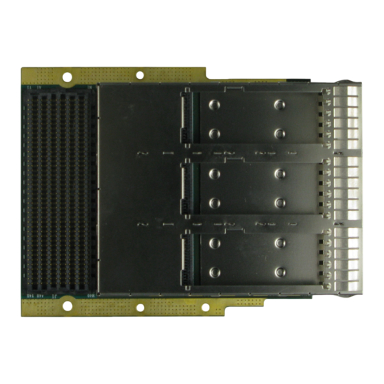
FMC-PLUS-QSFP-DD User Manual V1.0 - 20th July 2021 1.1 References & Specifications VITA 57.4 FMC+ Standard Specification Table 1 : References FMC+ 3xQSFP-DD Figure 3 : FMC-PLUS-QSFP-DD Top Side Features Page 2 Introduction ad-ug-1404_v1_0.pdf... -
Page 7: High Speed Serial Io (Hssio)
This enables support for a multitude of high speed serial IO communication protocols. 2.2 Connectors The QSFP DD connectors on the FMC-PLUS-QSFP-DD offers the user a wide selection of interconnect schemes that break out the multi-gigabit transceivers on the FPGA. -
Page 8: Installation
FMC+. The FMC-PLUS-QSFP-DD it should be removed in a certain way for the FMC+ connector not to be damaged. Here is a video from Samtec showing the removal procedure of this kind of connectors: see https:// vimeo.com/158484280... -
Page 9: Appendix A Fmc+ Pin Assignments
FMC-PLUS-QSFP-DD User Manual V1.0 - 20th July 2021 Appendix A: FMC+ Pin Assignments Appendix A.1: Clock Signals FMC Signal FMC (J1) Function Function FMC (J1) FMC Signal GBTCLK0_M2C_P* USER_CLK_P USER_CLK_N GBTCLK0_M2C_N* GBTCLK1_M2C_P* USER_CLK_P USER_CLK_N GBTCLK1_M2C_N* GBTCLK2_M2C_P* USER_CLK_P USER_CLK_N GBTCLK2_M2C_N* GBTCLK3_M2C_P*... -
Page 10: Table
FMC-PLUS-QSFP-DD User Manual V1.0 - 20th July 2021 FMC Signal FMC (J1) Function Function FMC (J1) FMC Signal DP10_M2C_P QSFP_1_RX_P2 | QSFP_1_TX_P2 DP10_C2M_P DP10_M2C_N QSFP_1_RX_N2 | QSFP_1_TX_N2 DP10_C2M_N DP11_M2C_P QSFP_1_RX_P3 | QSFP_1_TX_P3 DP11_C2M_P DP11_M2C_N QSFP_1_RX_N3 | QSFP_1_TX_N3 DP11_C2M_N DP12_M2C_P QSFP_1_RX_P4 | QSFP_1_TX_P4... -
Page 11: Appendix B Alpha Data Gpio Pin Assignments
FMC-PLUS-QSFP-DD User Manual V1.0 - 20th July 2021 Appendix B: Alpha Data GPIO Pin Assignments FMC Signal FMC (J1) Function LA02_P QSFP_0_SCL LA03_P QSFP_0_SDA LA04_P QSFP_0_RST_L LA05_P QSFP_0_LPMODE LA06_P QSFP_0_INT_L LA07_P QSFP_0_MODPRS_L LA08_P QSFP_1_SCL LA09_P QSFP_1_SDA LA010_P QSFP_1_RST_L LA011_P QSFP_1_LPMODE... - Page 12 FMC-PLUS-QSFP-DD User Manual V1.0 - 20th July 2021 Revision History Date Revision Changed By Nature of Change Initial Release 20 Jul 2021 A. Kapouranis Address: Suite L4A, 160 Dundee Street, Address: 10822 West Toller Drive, Suite 250 Edinburgh, EH11 1DQ, UK...
Need help?
Do you have a question about the FMC-PLUS-QSFP-DD and is the answer not in the manual?
Questions and answers