Table of Contents
Advertisement
Quick Links
www.ti.com
User's Guide
ADCxxDJxx00RF/SE Evaluation Module
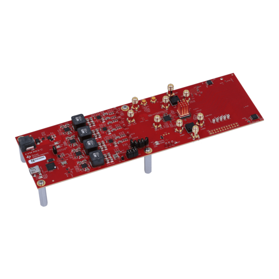
The ADCxxDJxx00RFEVM/SEEVM is an evaluation board used to evaluate the ADC12DJ5200RF,
ADC12DJ4000RF, ADC08DJ5200RF, ADC12DJ5200SE analog-to-digital converters (ADC) from Texas
Instruments. The ADC12DJ5200RF and SE is a dual-channel, 12/08-bit ADC, capable of operating at sampling
rates up to 5.2 and 4 Giga-samples per second (GSPS) in dual-channel mode, or 10.4 and 8 GSPS in single-
channel mode. The ADC12DJ5200RF/SE, ADC12DJ4000RF, ADC08DJ5200RF output data is transmitted over
a standard JESD204C high-speed serial interface. This evaluation board also includes the following important
features:
•
Transformer-coupled signal input network allowing a single-ended signal source from 500 kHz to
9 GHz. ADC12DJ5200SE has an internal balun in the ADC chip.
•
The LMX2594 clock synthesizer generates the ADC sampling clock
•
The LMK04828, LMK61E2 and LMX2594 onboard system clock generator generates SYSREF and FPGA
reference clocks for the high-speed serial interface
•
Transformer-coupled clock input network to test the ADC performance with an external low-noise clock
source
•
LM95233 temperature sensor
•
High-speed serial data output over a High Pin Count FMC+ interface connector
To improve signal routing quality, serial lane polarity is inverted with respect to the standard FMC
VITA-57 signal mapping. Signal mapping and polarity is shown in
•
Device register programming through USB connector and FTDI USB-to-SPI bus translator
SLAU640B – APRIL 2019 – REVISED MARCH 2023
Submit Document Feedback
ABSTRACT
Note
Copyright © 2023 Texas Instruments Incorporated
Table
8-1).
ADCxxDJxx00RF/SE Evaluation Module
1
Advertisement
Table of Contents

Related Manuals for Texas Instruments ADC DJ 00SE Series


Summary of Contents for Texas Instruments ADC DJ 00SE Series
- Page 1 VITA-57 signal mapping. Signal mapping and polarity is shown in Table 8-1). • Device register programming through USB connector and FTDI USB-to-SPI bus translator SLAU640B – APRIL 2019 – REVISED MARCH 2023 ADCxxDJxx00RF/SE Evaluation Module Submit Document Feedback Copyright © 2023 Texas Instruments Incorporated...
-
Page 2: Figure 1-1. Evm Orientation
ADC12DJ5200RF EVM top side with ADC12DJ5200RF EVM bottom side without heat sink installed heat sink installed Copyright © 2016, Texas Instruments Incorporated Figure 1-1. EVM Orientation The digital data from the ADCxxDJxx00RFEVM/SEEVM board is quickly and easily captured with the TSW14J57EVM data capture boards. -
Page 3: Table Of Contents
Rohde & Schwarz GmbH & Co. All trademarks are the property of their respective owners. SLAU640B – APRIL 2019 – REVISED MARCH 2023 ADCxxDJxx00RF/SE Evaluation Module Submit Document Feedback Copyright © 2023 Texas Instruments Incorporated... -
Page 4: Equipment
( J17 ) Mini USB Connector +12V DC ( J20 ) ( J14 ) Copyright © 2016, Texas Instruments Incorporated Figure 2-1. EVM Feature Locations ADCxxDJxx00RF/SE Evaluation Module SLAU640B – APRIL 2019 – REVISED MARCH 2023 Submit Document Feedback Copyright © 2023 Texas Instruments Incorporated... - Page 5 GUI using JMODE and the sampling frequency (Fs) entered by the user. The reference clock generator and device clock generator must be frequency-locked using a common 10-MHz reference. SLAU640B – APRIL 2019 – REVISED MARCH 2023 ADCxxDJxx00RF/SE Evaluation Module Submit Document Feedback Copyright © 2023 Texas Instruments Incorporated...
-
Page 6: Setup Procedure
2. Confirm that the power switch for the ADC12DJ5200EVMs power supply is in the off position. Connect the power cable to a 12-V DC (minimum 2 A) power supply. Make sure the proper supply polarity by confirming ADCxxDJxx00RF/SE Evaluation Module SLAU640B – APRIL 2019 – REVISED MARCH 2023 Submit Document Feedback Copyright © 2023 Texas Instruments Incorporated... - Page 7 1. Turn on the 12-V power supply to power up the EVM. 2. Connect the EVM to the PC with the mini-USB cable. SLAU640B – APRIL 2019 – REVISED MARCH 2023 ADCxxDJxx00RF/SE Evaluation Module Submit Document Feedback Copyright © 2023 Texas Instruments Incorporated...
- Page 8 Turn on the RF signal output of the signal generator connected to VIN. If external clocking is used, turn on the RF signal outputs connected to DEVCLK and Reference clock. ADCxxDJxx00RF/SE Evaluation Module SLAU640B – APRIL 2019 – REVISED MARCH 2023 Submit Document Feedback Copyright © 2023 Texas Instruments Incorporated...
-
Page 9: Figure 3-2. Configuration Gui Evm Tab
The max clock rate supported by ADC12DJ4000RF is 4000 MHz and only 8-bit mode are suppored by ADC08DJ5200RF. All the 12-bit and 15-bit modes are disabled on ADC08DJ5200RF. Figure 3-2. Configuration GUI EVM Tab SLAU640B – APRIL 2019 – REVISED MARCH 2023 ADCxxDJxx00RF/SE Evaluation Module Submit Document Feedback Copyright © 2023 Texas Instruments Incorporated... -
Page 10: Figure 3-3. Configuration Gui Adc Control
See the ADC12DJ5200RF/SE device data sheet, (SLVSEN9) for details regarding the necessary calibration sequence. 3. To enable background calibration, use the following steps: ADCxxDJxx00RF/SE Evaluation Module SLAU640B – APRIL 2019 – REVISED MARCH 2023 Submit Document Feedback Copyright © 2023 Texas Instruments Incorporated... - Page 11 SLAU640B – APRIL 2019 – REVISED MARCH 2023 ADCxxDJxx00RF/SE Evaluation Module Submit Document Feedback Copyright © 2023 Texas Instruments Incorporated...
-
Page 12: Figure 3-4. High Speed Data Converter Pro (Hsdc) Gui
The HSDC Pro GUI will calculate the ADC Output Data Rate based on these inputs. The Fundamental and Harmonic frequency locations will also be calculated and identified in the FFT display. ADCxxDJxx00RF/SE Evaluation Module SLAU640B – APRIL 2019 – REVISED MARCH 2023 Submit Document Feedback Copyright © 2023 Texas Instruments Incorporated... -
Page 13: Figure 3-5. Additional Device Parameters Dialog Box
Setup Procedure Figure 3-5. Additional Device Parameters Dialog Box SLAU640B – APRIL 2019 – REVISED MARCH 2023 ADCxxDJxx00RF/SE Evaluation Module Submit Document Feedback Copyright © 2023 Texas Instruments Incorporated... -
Page 14: Device Configuration
JESD204C settings. Once the settings are changed, re-enable the JESD204 block. 4.2 Tab Organization Control of the ADC device features are available in the EVM, Control, JESD204C, NCO Configuration tabs. ADCxxDJxx00RF/SE Evaluation Module SLAU640B – APRIL 2019 – REVISED MARCH 2023 Submit Document Feedback Copyright © 2023 Texas Instruments Incorporated... -
Page 15: Figure 4-1. Low-Level Register Control Tab
Perform a generic read or write command to the device shown in the Block drop-down box using the read or write register buttons address and write data information Figure 4-1. Low-Level Register Control Tab SLAU640B – APRIL 2019 – REVISED MARCH 2023 ADCxxDJxx00RF/SE Evaluation Module Submit Document Feedback Copyright © 2023 Texas Instruments Incorporated... -
Page 16: Troubleshooting The Adc12Dj5200Rfevm/Seevm
Verify that bandpass filters are used in the clock and input signal paths and that low-noise signal sources are used. ADCxxDJxx00RF/SE Evaluation Module SLAU640B – APRIL 2019 – REVISED MARCH 2023 Submit Document Feedback Copyright © 2023 Texas Instruments Incorporated... -
Page 17: References
FTDI USB to Serial Driver Installation Manual (www.ftdichip.com/Support/Documents/InstallGuides.htm) 6.2 TSW14J57EVM Operation Refer to the TSW14J57EVM user guide for configuration and status information. SLAU640B – APRIL 2019 – REVISED MARCH 2023 ADCxxDJxx00RF/SE Evaluation Module Submit Document Feedback Copyright © 2023 Texas Instruments Incorporated... -
Page 18: Hsdc Pro Settings For Optional Adc Device Configuration
The ADC12DJ5200RFEVM/SEEVM can be clocked using 3 different methods: external clock option, onboard clock option and external reference clock option. ADCxxDJxx00RF/SE Evaluation Module SLAU640B – APRIL 2019 – REVISED MARCH 2023 Submit Document Feedback Copyright © 2023 Texas Instruments Incorporated... -
Page 19: Figure 7-1. Adc12Dj5200Rfevm/Seevm Clocking System Block Diagram
SYSREF SYSREF CLKIN0 32.5 MHz SDCLKx SDCLKx FPGA_SYSREF External Clock CLKIN1 DCLKx FPGA_CLK[3:0] Figure 7-1. ADC12DJ5200RFEVM/SEEVM Clocking System Block Diagram SLAU640B – APRIL 2019 – REVISED MARCH 2023 ADCxxDJxx00RF/SE Evaluation Module Submit Document Feedback Copyright © 2023 Texas Instruments Incorporated... -
Page 20: Figure 7-2. Onboard Clocking System Block Diagram
SDCLKx SYSREFREQ RFOUTB SYSREF CLKIN0 SDCLKx SDCLKx FPGA_SYSREF Onboard Clock CLKIN1 DCLKx FPGA_CLK[3:0] Figure 7-2. Onboard Clocking System Block Diagram ADCxxDJxx00RF/SE Evaluation Module SLAU640B – APRIL 2019 – REVISED MARCH 2023 Submit Document Feedback Copyright © 2023 Texas Instruments Incorporated... -
Page 21: Figure 7-3. External Reference Clocking System Block Diagram
CLKIN0 32.5 MHz SDCLKx External SDCLKx FPGA_SYSREF Referencel Clock CLKIN1 DCLKx FPGA_CLK[3:0] Figure 7-3. External Reference Clocking System Block Diagram SLAU640B – APRIL 2019 – REVISED MARCH 2023 ADCxxDJxx00RF/SE Evaluation Module Submit Document Feedback Copyright © 2023 Texas Instruments Incorporated... -
Page 22: Figure 7-4. External Clock Configuration
HSDC Pro Settings for Optional ADC Device Configuration www.ti.com Figure 7-4. External Clock Configuration ADCxxDJxx00RF/SE Evaluation Module SLAU640B – APRIL 2019 – REVISED MARCH 2023 Submit Document Feedback Copyright © 2023 Texas Instruments Incorporated... -
Page 23: Figure 7-5. Onboard Clocking Configuration
HSDC Pro Settings for Optional ADC Device Configuration Figure 7-5. Onboard Clocking Configuration SLAU640B – APRIL 2019 – REVISED MARCH 2023 ADCxxDJxx00RF/SE Evaluation Module Submit Document Feedback Copyright © 2023 Texas Instruments Incorporated... -
Page 24: Signal Routing
Y18,Y19 DP14_M2C_INV Y22,Y23 DP15_M2C_INV Red items with _INV in the signal name are inverted with respect to standard FMC polarity. ADCxxDJxx00RF/SE Evaluation Module SLAU640B – APRIL 2019 – REVISED MARCH 2023 Submit Document Feedback Copyright © 2023 Texas Instruments Incorporated... -
Page 25: A Analog Inputs
5200SE = N/A INBP(J6), INBM(J8) Differential INAP, INAM, INBP, INBM 0 Ω 5200SE = N/A Figure A-1. Analog Input Path SLAU640B – APRIL 2019 – REVISED MARCH 2023 ADCxxDJxx00RF/SE Evaluation Module Submit Document Feedback Copyright © 2023 Texas Instruments Incorporated... -
Page 26: Figure A-2. 3 Db Attenuation Pad
A 3dB attenuation pad is added between the inputs and the ADC. The 3 dB pad helps with the flatness of the frequency response. Figure A-2. 3 dB attenuation pad ADCxxDJxx00RF/SE Evaluation Module SLAU640B – APRIL 2019 – REVISED MARCH 2023 Submit Document Feedback Copyright © 2023 Texas Instruments Incorporated... -
Page 27: B Jumpers And Leds
Changed the abstract to include additional devices................... • Added a Note to Open the ADC12DJ5200RFEVM/SEEVM GUI and Program the ADC and Clocks ....SLAU640B – APRIL 2019 – REVISED MARCH 2023 ADCxxDJxx00RF/SE Evaluation Module Submit Document Feedback Copyright © 2023 Texas Instruments Incorporated... - Page 28 STANDARD TERMS FOR EVALUATION MODULES Delivery: TI delivers TI evaluation boards, kits, or modules, including any accompanying demonstration software, components, and/or documentation which may be provided together or separately (collectively, an “EVM” or “EVMs”) to the User (“User”) in accordance with the terms set forth herein.
- Page 29 www.ti.com Regulatory Notices: 3.1 United States 3.1.1 Notice applicable to EVMs not FCC-Approved: FCC NOTICE: This kit is designed to allow product developers to evaluate electronic components, circuitry, or software associated with the kit to determine whether to incorporate such items in a finished product and software developers to write software applications for use with the end product.
- Page 30 www.ti.com Concernant les EVMs avec antennes détachables Conformément à la réglementation d'Industrie Canada, le présent émetteur radio peut fonctionner avec une antenne d'un type et d'un gain maximal (ou inférieur) approuvé pour l'émetteur par Industrie Canada. Dans le but de réduire les risques de brouillage radioélectrique à...
- Page 31 www.ti.com EVM Use Restrictions and Warnings: 4.1 EVMS ARE NOT FOR USE IN FUNCTIONAL SAFETY AND/OR SAFETY CRITICAL EVALUATIONS, INCLUDING BUT NOT LIMITED TO EVALUATIONS OF LIFE SUPPORT APPLICATIONS. 4.2 User must read and apply the user guide and other available documentation provided by TI regarding the EVM prior to handling or using the EVM, including without limitation any warning or restriction notices.
- Page 32 Notwithstanding the foregoing, any judgment may be enforced in any United States or foreign court, and TI may seek injunctive relief in any United States or foreign court. Mailing Address: Texas Instruments, Post Office Box 655303, Dallas, Texas 75265 Copyright © 2023, Texas Instruments Incorporated...
- Page 33 TI products. TI’s provision of these resources does not expand or otherwise alter TI’s applicable warranties or warranty disclaimers for TI products. TI objects to and rejects any additional or different terms you may have proposed. IMPORTANT NOTICE Mailing Address: Texas Instruments, Post Office Box 655303, Dallas, Texas 75265 Copyright © 2023, Texas Instruments Incorporated...
Need help?
Do you have a question about the ADC DJ 00SE Series and is the answer not in the manual?
Questions and answers