
Related Manuals for ADLINK Technology NuPRO-796 Series


Summary of Contents for ADLINK Technology NuPRO-796 Series
- Page 1 NuPRO-796 ETX PICMG 1.0 Half-Size SBC User’s Manual Manual Rev. 2.00 Revision Date: August 20, 2006 Part No: 50-13051-1000 Advance Technologies; Automate the World.
- Page 2 Copyright 2006 ADLINK TECHNOLOGY INC. All Rights Reserved. The information in this document is subject to change without prior notice in order to improve reliability, design, and function and does not represent a commitment on the part of the manufacturer.
- Page 3 Getting Service from ADLINK Customer Satisfaction is top priority for ADLINK Technology Inc. Please contact us should you require any service or assistance. ADLINK TECHNOLOGY INC. Web Site: http://www.adlinktech.com Sales & Service: Service@adlinktech.com TEL: +886-2-82265877 FAX: +886-2-82265717 Address: 9F, No. 166, Jian Yi Road, Chungho City,...
-
Page 5: Table Of Contents
Table of Contents 1 Introduction ................ 1 Product Overview ..............1 Unpacking Checklist ............1 Specifications............... 2 Display (CRT + LVDS) ............ 3 Multi I/O ................3 Audio ................3 LAN ................. 4 Mechanical and Environmental ........4 NuPRO-796 Functional Diagram ......... 5 NuPRO-796 Mechanical Diagram ........ - Page 6 I/O Map ................22 Interrupt Request (IRQ) Lines..........23 PCI Configuration Space Map ........... 24 PCI Interrupt Routing Map ..........24 System Management Bus and I2C Bus ......24 4 Phoenix Award BIOS ............25 Description ................. 25 Main Menu ................. 26 Standard CMOS Features ..........
- Page 7 Master/Slave PIO ............38 IDE Primary Master/Slave UDMA ......... 39 IDE HDD Block Mode ........... 39 Onboard Serial Port 1 & 2 ..........39 UART Mode Select ............39 LPT1 Setting / FDD ............39 ECP Mode Use DMA ............ 39 PnP/PCI Configurations.............
- Page 8 List of Figures Figure 1-1: NuPRO-796 Block Diagram........5 Figure 1-2: NuPRO-796 Carrier Board Layout......6 List of Figures...
-
Page 9: Introduction
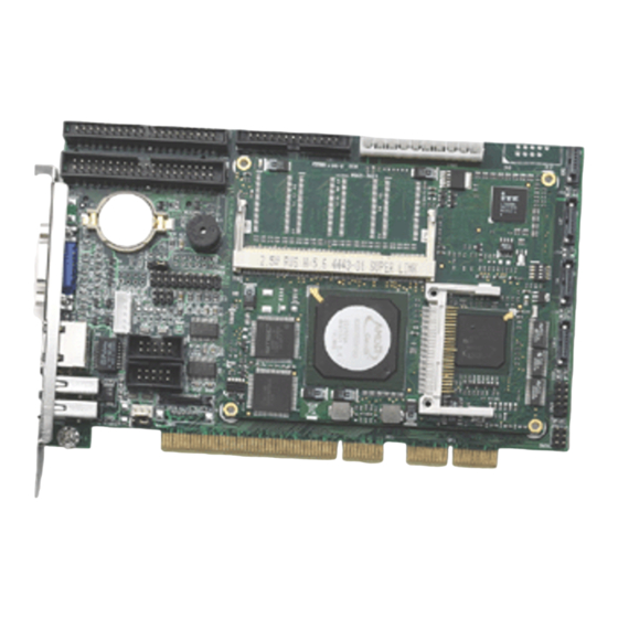
Introduction 1.1 Product Overview The NuPRO-796 ETX-based single board computer is comprised of the ProCB-796, a PICMG 1.0 compliant half-size carrier board, and the ETX-GX2 ETX module. The ProCB-796 carrier board includes common PC peripheral I/O interfaces such as serial and parallel ports, keyboard/mouse, Ethernet, IDE, VGA, and audio. -
Page 10: Specifications
Included Items NuPRO-796 carrier board with ETX-GX2 module This user manual Printer and COM port cable bracket ATA-100 cable (x1) SATA cable kit (x2) Note: The packaging of the NuPRO-796 OEM version with non-standard configuration, functionality, or package may vary according to different configuration re- quests. -
Page 11: Display (Crt + Lvds)
IDE hard drive is required for installation of operation system! Hardware Monitor: integrated in SMSC SCH3112 monitors supply voltages and CPU temperature Watchdog Timer: 255-level timer generates RESET Expansion: 16-bit ISA and 32-bit PCI 2.1 1.3.1 Display (CRT + LVDS) Chipset: Integrated AMD Geode™... -
Page 12: Lan
1.3.4 LAN Chipset: Intel® 82551ER Interface: 10BASE-T/ 100BASE-TX with TCP/UDP/IP checksum offloading 1.3.5 Mechanical and Environmental Power Requirement: (+5V only) : 4 Watt typical with GX533 and 128 MB soldered DDR266 Operating Temperature: 0 to 60°C (32 to 140°F) Relative Humidity: up to 90% @ 55°C ETX Board Dimensions: 95 mm x 114 mm (3.7"... -
Page 13: Nupro-796 Functional Diagram
1.4 NuPRO-796 Functional Diagram Figure 1-1: NuPRO-796 Block Diagram Introduction... -
Page 14: Nupro-796 Mechanical Diagram
1.5 NuPRO-796 Mechanical Diagram Figure 1-2: NuPRO-796 Carrier Board Layout Introduction... -
Page 15: Connectors And Jumpers
Connectors and Jumpers This chapter will familiarize the user with the connectors on the NuPRO-796. 2.1 Connector Pin Assignments Detailed descriptions and pin-outs for each connector are given in the following section. Connectors and Jumpers... -
Page 16: Vga Connector (Cn10)
2.1.1 VGA Connector (CN10) Signal Name Pin Pin Signal Name Green Blue N.C. N.C. DDCDAT HSYNC VSYNC DDCCLK 2.1.2 USB Connector (CN17, CN22) SIGNAL USB- USB+ Ground 2.1.3 Keyboard and Mouse (CN11) Signal Name Keyboard Data Keyboard Clock Mouse Data Mouse Clock Power Ground... -
Page 17: Com Pin Header (Cn15, Cn16)
2.1.4 COM Pin Header (CN15, CN16) RS-232 DCD, Data carrier detect RXD, Receive data TXD, Transmit data DTR, Data terminal ready GND, ground DSR, Data set ready RTS, Request to send CTS, Clear to send RI, Ring indicator 2.1.5 Parallel Port (CN1) Signal Name Signal Name Line printer strobe... -
Page 18: Ide (Cn4)
2.1.6 IDE (CN4) Signal Name Signal Name Reset IDE IDE Data 7 IDE Data 8 IDE Data 6 IDE Data 9 IDE Data 5 IDE Data 10 IDE Data 4 IDE Data 11 IDE Data 3 IDE Data 12 IDE Data 2 IDE Data 13 IDE Data 1 IDE Data 14... -
Page 19: Usb Pin Header (Cn24)
2.1.7 USB Pin Header (CN24) Signal Name Signal Name USB1_VCC USB2_VCC USB1- USB2- USB1+ USB2+ 2.1.8 Serial ATA Connector (CN5, CN7, CN9, CN14) Signal Name Connectors and Jumpers... -
Page 20: Ldvs Connector (Cn19)
2.1.9 LDVS Connector (CN19) Signal Name Signal Name Txout2# Txout2 Txclk# Txout0# Txclk Txout0 Txout3# Txout1# Txout3 Txout1 Panel Detect Connectors and Jumpers... -
Page 21: Miscellaneous Connector (Cn18)
2.1.10 Miscellaneous Connector (CN18) Signal Name Signal Name PW_LED+ BUZZER PW_LED- KB_LOCK POWER LED SPEAKER (BUZZER) PW_GD KEYBOARD LOCK RESET BOTTON HDD_LED- ATX POWER HDD LED CONN. PS_ON HDD_LED+ POWER BOTTON 5VSB PW_BTN PME# 2.1.11 Fan Connector (CN20) Signal Name +12V 2.1.12 Audio-Out Pin Header (CN26) Signal Name... -
Page 22: Atx Power Connector (Cn29)
2.1.13 ATX Power Connector (CN29) Signal Signal +3.3V +3.3V +3.3V -12V PS_ON# PWRGOOD STB5V +12V 2.1.14 ETX Connector Connectors and Jumpers... -
Page 23: Etx X1 Connector (Pci Bus, Usb, Audio)
2.1.15 ETX X1 Connector (PCI Bus, USB, Audio) Signal Name Signal Name PCICLK3 PCICLK4 PCICLK1 PCICLK2 REQ3# GNT3# GNT2# REQ2# GNT1# REQ1# GNT0# RESERVED SERIRQ REQ0# C/BE0# AD10 LINEIN_L AD11 MICIN AD12 LINEIN_R AD13 AVCC AD14 LINEOUT_L AD15 AGND C/BE1# LINEOUT_R SERR# PERR#... -
Page 24: Etx X2 Connector (Isa Bus)
2.1.16 ETX X2 Connector (ISA Bus) Signal Name Signal Name SD14 SD15 SD13 MASTER# SD12 DREQ7 SD11 DACK7# SD10 DREQ6 DACK6# DREQ5 MEMW# DACK5# MEMR# DREQ0 LA17 DACK0# LA18 IRQ14 LA19 IRQ15 LA20 IRQ12(1) LA21 IRQ11 LA22 IRQ10 LA23 IO16# SBHE# M16# BALE... -
Page 25: Etx X3 Connector (Video, Com, Misc. I/O)
2.1.17 ETX X3 Connector (Video, COM, misc. I/O) Signal Name Signal Name BLUE HSYNC GREEN VSYNC DDC2B_CLK PAL_DETECT# DDC2B_DAT LCDDO16 LCDDO18 LCDDO17 LCDDO19 LCDDO13 LCDDO15 LCDDO12 LCDDO14 LCDDO8 LCDDO11 LCDDO9 LCDDO10 LCDDO4 LCDDO7 LCDDO5 LCDDO6 LCDDO1 LCDDO3 LCDDO0 LCDDO2 JILI_DAT JILI_CLK BLON# BIASON... -
Page 26: Etx X4 Connector (Ethernet, Ide, Power, I2C & Smb)
2.1.18 ETX X4 Connector (Ethernet, IDE, Power, I C & SMB) Signal Name Signal Name 5V_SB PWGIN PS_ON SPEAKER PWRBTN# BATT KBINH LILED RSMRST# ACTLED ROMKBCS#(1) SPDLED EXT_PRG(1) I2CLK OVCR# GPCS#(1) EXTSMI# I2DAT SMBCLK SMBDATA SIDE_CS3# SMBALRT# SIDE_CS1# DASP_S(1) SIDE_A2 PIDE_CS3# SIDE_A0 PIDE_CS1#... -
Page 27: Jumper Settings
2.2 Jumper Settings 2.2.1 Panel Power Selection (JP3) Jumper Status +3.3V Connectors and Jumpers... - Page 28 Connectors and Jumpers...
-
Page 29: System Resources
System Resources 3.1 System Memory Map PCI and ISA interrupts supported by the GX2/CS5355 are as fol- lows: Address Range Address Range (hex) Size Description (decimal) 100000 - TOM N.A. Extended memory 1024 K - TOM 928 K - 1024 K E8000 - FFFFF 96 KB System BIOS... -
Page 30: I/O Map
3.3 I/O Map Address (hex) Size Description Available 0000 - 000F 16 bytes DMA controller 1 0020 - 0021 2 bytes Interrupt controller 1 0040 - 0043 4 bytes Counter/Timer 1 0060 1 byte Keyboard controller 0061 1 byte NMI, speaker control 0064 1 byte Keyboard controller... -
Page 31: Interrupt Request (Irq) Lines
3.4 Interrupt Request (IRQ) Lines Note: PIC Mode only ! IRQ# Typical Interrupt Resource Connected Available AT Timer N.A. Keyboard N.A. None N.A. COM2 IRQ3 via SERIRQ Note1 COM1 IRQ4 via SERIRQ Note1 Standard OpenHCD USB Host Controller IRQ5 via SERIRQ Floppy Drive Controller IRQ6 via SERIRQ Note1... -
Page 32: Pci Configuration Space Map
3.5 PCI Configuration Space Map Bus Number Device Number Function Number Routing Description internal Display Cntrlr INTA-INTD Network Cntrlr Internal IDE Cntrlr Internal Multimedia Device Internal USB 1.0/1.1 OHCI Cntrlr Internal USB 1.0/1.1 OHCI Cntrlr INTA-INTD PCI Bus Slot 1 INTA-INTD PCI Bus Slot 2 INTA-INTD... -
Page 33: Phoenix Award Bios
Phoenix Award BIOS 4.1 Description The module has a Phoenix Award PCI/ISA BIOS ver 6.0 for the system configuration. The Award BIOS setup program is designed to provide the maximum flexibility in configuring the system by offering various options which could be selected for end-user requirements. -
Page 34: Main Menu
4.2 Main Menu Standard CMOS Features. Use this menu for basic system configuration. Advanced BIOS Features. Use this menu to set the Advanced Features available on your system. Advanced Chipset Features. Change values in the chipset registers and optimize your system's performance. Integrated Peripherals.Use this menu to specify your set- tings for integrated peripherals. -
Page 35: Standard Cmos Features
4.3 Standard CMOS Features The main menu includes the following main setup categories. Recall that some systems may not include all entries. Date.The BIOS determines the day of the week from other date information; this field is for information only. Time. - Page 36 BIOS menu: Integrated Peripherals > Super I/O Device > LPT1 Set- ting / FDD This menu allows setup of LPT1 resources or disabling of LPT1 and setting the mode to FDD. After enabling the FDD, select the correct specifications for the diskette drive: None: No diskette drive installed 360K: 5-1/4 inch PC-type standard drive...
- Page 37 IDE Primary Master/Slave Items IDE HDD Auto-detection Press Enter Press Enter to auto-detect the HDD on this channel. If detection is successful, it fills the remaining fields on this menu. IDE Primary Master None/Auto/Manual Selecting 'manual' lets you set the remaining fields on this screen. Selects the type of fixed disk.
- Page 38 The following options are selectable only if the 'IDE Primary Mas- ter' item is set to 'Manual' Set the number of cylinders for Cylinder Min = 0 Max = 65535 this hard disk. Set the number of read/write Head Min = 0 Max = 255 heads **** Warning: Setting a value of Precomp...
-
Page 39: Advanced Bios Features
4.4 Advanced BIOS Features This section allows the user to configure the system for basic operation. The following features can be selected here: system default speed, boot-up sequence, keyboard operation, shadowing, security, and CPU Internal Cache/CPU External Cache. 4.4.1 CPU Internal Cache This function enables/disables CPU Internal Cache. -
Page 40: First/Second/Third Boot Device
POST. Options: Enabled: enables quick POST. Disabled: normal POST. 4.4.3 First/Second/Third Boot Device Pressing Enter brings up the Boot Device Menu. The BIOS attempts to load the operating system from the selected device. See menu for possible options 4.4.4 Boot Other Device When enabled, the BIOS will try to boot from second or third option if booting from first device fails. -
Page 41: Typematic Rate Setting
Normal: A pin in the keyboard controller controls GateA20 Fast: Lets chipset control GateA20 4.4.7 Typematic Rate Setting Key strokes repeat at a rate determined by the keyboard control- ler. When enabled, the typematic rate and typematic delay can be selected. -
Page 42: Console Redirection
4.4.12 Console Redirection Award's Preboot Agent provides you with console redirection to let you control a remote PC or embedded system via modem or direct serial connection at boot time. Choices: Enable, Disable. 4.4.13 Baudrate Select baud rate: 9600,19200, 38400, 57600 and 115200. 4.4.14 Agent Connect via Fixed to NULL (Null modem cable), no selection possible. -
Page 43: Agent Connect Via
The Baud Rate setting between module and monitoring computer must be the same. When different, a error message "Award Pre- boot Agent Installation Failed" will display when BIOS is building the connection between two computers. 4.4.20 Agent Connect via This field selects connection mode. Only supported is: NULL mode. -
Page 44: Advanced Chipset Features
4.5 Advanced Chipset Features 4.5.1 Video Memory Size The NuPRO-796 VGA controller uses a portion of system memory as video memory. The use of main system memory for video memory is called Unified Memory Architecture (UMA). The amount of system memory that can be assigned to the video controller is: None, 4 , 6, 8, 12 or 16 MB. -
Page 45: Onboard Audio
4.5.3 Onboard Audio Enable or Disable Phoenix Award BIOS... -
Page 46: Integrated Peripherals
4.6 Integrated Peripherals 4.6.1 OnChip IDE Channel 0/1 The chipset contains a PCI IDE interface with support for two IDE channels. Select Enabled to activate the primary IDE interface. Select Disabled to deactivate this interface 4.6.2 Master/Slave PIO The four IDE PIO (Programmed Input/Output) fields let you set a PIO mode (0-4) for each of the four IDE devices that the onboard IDE interface supports. -
Page 47: Ide Primary Master/Slave Udma
determines the best mode for each device. Choice: Auto, Mode 0, Mode 1, Mode 2, Mode 3, Mode 4. 4.6.3 IDE Primary Master/Slave UDMA Ultra DMA implementation is possible only if your IDE hard drive supports it and the operating environment includes a DMA driver. If your hard drive and your system software both support Ultra DMA, select Auto to enable BIOS support. -
Page 48: Pnp/Pci Configurations
4.7 PnP/PCI Configurations This section describes the configuring of the PCI bus system. PCI, or Personal Computer Inter¬connect, is a system which allows I/O devices to operate at speeds nearing the speed the CPU itself uses when communicating with its own special components. 4.7.1 Init Display First This item allows you to decide to activate either PCI Slot VGA con- troller or the integrated onboard VGA controller... -
Page 49: Resource Controlled By
caused such a serious conflict that the operating system cannot boot. 4.7.3 Resource Controlled By The Award Plug and Play BIOS can automatically configure all the boot and Plug-and-Play compatible devices. If Auto is selected, all interrupt requests (IRQ) and DMA assignment fields disappear, as the BIOS automatically assigns them. -
Page 50: Dma Resources
4.7.5 DMA Resources Legacy ISA for devices compliant with the original PC/AT bus specification, requiring a specific interrupt (such as IRQ4 for serial port 1). PCI/ISA PnP for devices that comply with the Plug and Play standard, whether designed for PCI or ISA bus architecture. architecture. -
Page 51: Memory Resources
4.7.6 Memory Resources The memory resource menu allows you to exclude memory from being used by the system. In the menu you can both set the start address as well as the memory length. Select a base address for the memory area used by any periph- eral that requires high memory. -
Page 52: Pc Health Status
This option is only very rarely needed. It should be left at "Dis- abled" unless a video device specifically requires the setting enabled upon installation. 4.8 PC Health Status 4.8.1 Current System Temp. Displays the current system temperature measured on the rear side of the module 4.8.2 Current CPU1 Temp. -
Page 53: Bios Post Messages
BIOS POST Messages If BIOS detects an error during the Power On Self-Test (POST), it will prompt the user by either sounding a beep code or displaying a message. If a message is displayed, it will be accompanied by: PRESS F1 TO CONTINUE, OR DEL TO ENTER SETUP 4.9.1 POST Beep Currently there are two kinds of beep codes in BIOS : This first beep code indicates that a video error has... - Page 54 DISKETTE DRIVES OR TYPES MISMATCH ERROR - RUN SETUP Type of diskette drive installed in the system is different from the CMOS definition. Run Setup to reconfigure the drive type correctly. DISPLAY SWITCH IS SET INCORRECTLY Display switch on the motherboard can be set to either mono- chrome or color.
- Page 55 PRESS A KEY TO REBOOT This will be displayed at the bottom screen when an error occurs that requires you to reboot. Press any key and the sys- tem will reboot. PRESS F1 TO DISABLE NMI, F2 TO REBOOT When BIOS detects a Non-Maskable Interrupt condition during boot, you can choose to disable the NMI and continue to boot, or you can reboot the system with NMI enabled.
-
Page 56: Bios Post Codes
4.10 BIOS POST Codes 4.10.1 Normal POST Codes POST (hex) Name Description OEM Specific-Cache control cache Processor Status (1FLAGS) Verification. Tests the follow- ing processor status flags: Carry, zero, sign, overflow, The BIOS sets each flag, verifies They are set, then turns each flag off and veri- Turn Off Chipset And CPU test fies it is off. - Page 57 POST (hex) Name Description OEM Specific- Display/Video Switch Handling so that Special Display Handling Switch Handling display switch errors never occurs OEM specific- Early shadow Early Shadow enable for fast boot External cache size detec- Cache presence tion test CMOS Check CMOS checkup If interrupt occurs in pro- Spurious...
- Page 58 POST (hex) Name Description Check the intergraty of the CheckSum Check ROM,BIOS and message Reserved Check Flash type and copy Auto detec EEPROM flash write/erase routines to 0F000h segments Reserved Check Cmos Circuitry and Cmos Check reset CMOS Reserved Program the chipset regis- Chipset Default load ters with CMOS values Reserved...
- Page 59 POST (hex) Name Description Reserved Reserved Reserved Final Initial KBC and setup KBC final Init BIOS data area Reserved Read CMOS location 14h to find out Interface type of Initialize Video video in use. Detect and Ini- tialize Video Adapter. Reserved Reserved Reserved...
- Page 60 POST (hex) Name Description Reserved Verify 8259 Channel 1 masked interrupts by alter- Test 8259-1 Mask Bits nately turning off and on the interrupt lines. Reserved Verify 8259 Channel 2 masked interrupts by alter- Test 8259-2 Mask Bits nately turning off and on the interrupt lines.
- Page 61 POST (hex) Name Description Test base memory from 256K to 640K and extended memory above 1MB using Test Base and Extended Mem- various patterns. NOTE: This test is skipped in EISA mode and can be skipped with ESC key in ISA mode.
- Page 62 POST (hex) Name Description Reserved Reserved Detect if mouse is present, Install Mouse initialize Initialize & mouse, install interrupt vec- tors. Reserved Special treatment to PS2 PS2 Mouse special Mouse port Reserved ACPI init ACPI sub-system initializing Reserved Setup Cache Controller Initialize cache controller.
- Page 63 POST (hex) Name Description Detect & Initialize Math Copro- Initialize math coprocessor. cessor Reserved HDD Check for Write protection HDD check out Reserved Reserved Check POST error and dis- POST error check play them and ask for user intervention Reserved Reserved Ask password security Security Check...
- Page 64 POST (hex) Name Description Reserved Reserved Reserved Read and store boot partition Boot Medium detection head and cylinders values in Final init for last micro details Final Init before boot Set system speed for boot Special KBC patch Setup NumLock status according to Setup Set low stack Boot via INT Boot Attempt...
-
Page 65: Watchdog Timer
Watchdog Timer The NuPRO-796 implements a watchdog timer embedded in the LPC based SMSC SCH3112 Super I/O controller. The Watchdog timer contains of a one-second/minute resolution down counter. The Watchdog output is connected to "RESET". When the system hangs up without software re-trigger, the system will be reset. - Page 66 void main() unsigned charTimeOut_Val=0,Mode=3; printf("SMSC SIO3112 Watch-Dog Function test utility.\n\n"); while((Mode > 2)||(Mode==0)) printf("Please select the unit(1:Min, 2:Sec):"); scanf("%d",&Mode); switch(Mode) case 1: while((TimeOut_Val==0)||(TimeOut_Val > 255)) printf("Min.(1- 255):");scanf("%d",&TimeOut_Val); break; case 2: while((TimeOut_Val==0)||(TimeOut_Val > 255)) printf("Sec.(1- 255):");scanf("%d",&TimeOut_Val); break; if(Mode==1) Mode=0; else _asm Watchdog Timer...
- Page 67 Mode=0x80; dx,0x847 //WDT_EN_REG al,0x0E //WDT enable and invert dx,al 0xeb,al dx,0x865 //WDT_MOD_REG al,Mode dx,al 0xeb,al dx,0x866 //WDT_VAL_REG al,TimeOut_Val dx,al Watchdog Timer...
- Page 68 Watchdog Timer...
-
Page 69: Appendix
Appendix 6.1 Onboard DIP switch 6.1.1 Location & Function A board configuration DIP switch is located on the right side of the board just over the CF card socket The DIP switch can be used to configure Master/Slave mode for the onboard CF card or configure CRT or TFT mode for display. -
Page 70: Flat Panel / Crt Settings
6.1.3 Flat Panel / CRT settings TFT LVDS mode or CRT mode can be selected here. Note that TFT LVDS can support dual and single channel LVDS. Switch CRT Mode TFT (LVDS) mode Dual channel LVDS Single channel LVDS Switch 3 is not used but should always bet set to ON! - Page 71 Important Safety Instructions Please read and follow all instructions marked on the product and in the documentation before operating the system. Retain all safety and operating instructions for future use. Please read these safety instructions carefully. Please keep this User’s Manual for future reference. The equipment should be operated in an ambient tempera- °...
- Page 72 Openings in the case are provided for ventilation. Do not block or cover these openings. Make sure there is adequate space around the system for ventilation when setting up the work area. Never insert objects of any kind into the ventila- tion openings.
- Page 73 Warranty Policy Thank you for choosing ADLINK. To understand your rights and enjoy all the after-sales services we offer, please read the follow- ing carefully. 1. Before using ADLINK’s products please read the user man- ual and follow the instructions exactly. When sending in damaged products for repair, please attach an RMA appli- cation form which can be downloaded from: http:// rma.adlinktech.com/policy/.
- Page 74 3. Our repair service is not covered by ADLINK's guarantee in the following situations: Damage caused by not following instructions in the User's Manual. Damage caused by carelessness on the user's part dur- ing product transportation. Damage caused by fire, earthquakes, floods, lightening, pollution, other acts of God, and/or incorrect usage of voltage transformers.
Need help?
Do you have a question about the NuPRO-796 Series and is the answer not in the manual?
Questions and answers