
Related Manuals for ADLINK Technology NuPRO-841


Summary of Contents for ADLINK Technology NuPRO-841
- Page 1 NuPRO-841 Full-Size SBC User’s Manual Manual Rev. 2.00 Revision Date: January 3, 2005 Part No: Advance Technologies; Automate the World.
- Page 2 Copyright 2005 ADLINK TECHNOLOGY INC. All Rights Reserved. The information in this document is subject to change without prior notice in order to improve reliability, design, and function and does not represent a commitment on the part of the manufacturer.
- Page 3 Getting Service from ADLINK Customer Satisfaction is top priority for ADLINK Technology Inc. Please contact us should you require any service or assistance. ADLINK TECHNOLOGY INC. Web Site: http://www.adlinktech.com Sales & Service: Service@adlinktech.com TEL: +886-2-82265877 FAX: +886-2-82265717 Address: 9F, No. 166, Jian Yi Road, Chungho City,...
-
Page 5: Table Of Contents
Table of Contents Table of Contents..............i List of Tables................. vii List of Figures ................ ix 1 Introduction ................ 1 Unpacking Checklist ............1 Included Items ..............2 Optional Items ..............3 Description................4 Features................4 Hardware Monitoring ............5 I/O Shield Connector ............ - Page 6 PnP / PCI Configuration ..........36 PC Health Status ............36 Frequency / Voltage Control ......... 36 Load Fail-Safe Defaults ..........37 Load Optimized Defaults ..........37 Supervisor / User Password ......... 37 Save & Exit Setup ............37 Exit Without Save ............37 Standard CMOS Features ..........
- Page 7 Gate A20 Option ............44 Typematic Rate Setting ..........44 Typematic Rate (Chars/Sec) ........44 Typematic Delay (Msec) ..........44 Security Option ............. 44 APIC Mode ..............45 MPS Version Control For OS ........45 OS Select For DRAM > 64MB ........45 Report No FDD For WIN95 ...........
- Page 8 IR Transmission Delay ..........52 UR2 Duplex Mode ............52 Use IR Pins ..............52 Onboard Parallel Port ........... 52 Parallel Port Mode ............52 EPP Mode Select ............52 ECP Mode Use DMA ............ 52 PWRON After PWR-Fail ..........53 Power Management Setup ..........
- Page 9 Shutdown Temperature ..........60 3.11 Frequency/Voltage Control ..........61 CPU Clock Ratio ............61 Auto Detect PCI CLK ............ 61 Spread Spectrum ............61 3.12 Load Fail-Safe Defaults ............. 62 3.13 Load Optimized Defaults ........... 62 3.14 Supervisor/User Password Setting ........62 3.15 Exit Selecting ..............
-
Page 10: List Of Tables
List of Tables Table 2-1: Jumper Settings ............14 Table 2-2: JP1: COM Port Setting ........... 14 Table 2-3: JP2: Clear CMOS ........... 15 Table 2-4: JP3: Watchdog Timer ..........15 Table 2-5: Connector Locations ..........17 Table 2-6: CN1: System Panel Indicator Connector ....18 Table 2-7: CN2: Primary IDE Connector ........ - Page 11 List of Figures Figure 1-1: I/O Bracket Layout............. 5 Figure 1-2: System Block Diagram ..........6 Figure 2-1: CPU Socket ............... 9 Figure 2-2: Heat Sink & Retention Module Installation ....10 Figure 2-3: DIMM Memory and 184-pins Socket ....... 11 Figure 2-4: Memory Installation ..........
-
Page 13: Introduction
Introduction 1.1 Unpacking Checklist Check the shipping carton for any damage. If the shipping carton and contents are damaged, notify the dealer for a replacement. Retain the shipping carton and packing materials for inspection by the dealer. Obtain authorization before returning any product to ADLINK. -
Page 14: Included Items
Included Items Installation Guide Single Board Computer Floppy ribbon cable ATA-66/100 HDD ribbon cable Print ribbon cable COM2 ribbon cable Driver CD K/B & M/S Y type cable K/B-M/S extend to BP cable ATX power control cable (5-pin to 6-pin) (4-pin to 4-pin) Introduction... -
Page 15: Optional Items
Optional Items IP-ALCS20 Audio card Audio 9-pins round cable Note: The packaging of the OEM version with NuPRO-841 non-standard configuration, functionality, or package may vary according to different configuration requests. CAUTION: The single board computer must be pro- NuPRO-841 tected from static discharge and physical shock. Never remove any of the socketed parts except at a static-free workstation. -
Page 16: Description
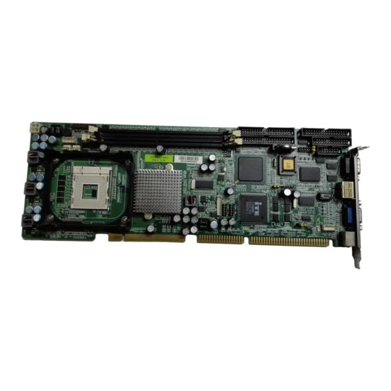
1.2 Description The NuPRO-841 single board computer is optimized for socket 478 FC-PGA Intel Pentium 4 (Northwood) processors up to 3.06GHz and Intel Pentium 4 (Prescott) processors up to 2.8 GHz, supporting 533 / 400MHz Front Side Bus. The memory can accommodate up to 2GB DDR 266 / 333 SDRAM. -
Page 17: Hardware Monitoring
Hardware Monitoring Hardware monitoring allows you to monitor various aspects of your systems operations and status, including CPU temperature, voltage, and fan RPM. I/O Shield Connector The SBC is equipped with an I/O bracket. Please use the appropri- ate I/O shield (Figure 1.1). Figure 1-1: I/O Bracket Layout NuPRO-841Overview Chipset: 845GV... -
Page 18: System Block Diagram
System Block Diagram P4 Socket 478-pins Support Prescott Code Clock Processor ADDR CTRL DATA GMCH (845GV) DDR266/333 X2 760 FC-BGA IDE Primary ATA100 10/100 T-Base IDE Secondary ICH4 82562ET 421 BGA USB Port 1/2 USB Port 3/4 PCI BUS ISA BUS Super I/O iTE Bridge W83627HF... -
Page 19: Specifications
1.4 Specifications Processor: Socket 478-pins, for Intel Pentium 4/ Celeron processors (Northwood / Prescott) Chipset: Intel® 845GV + ICH4 AGPset Front Side Bus: 400 / 533 MHz DRAM Module: 184-pins DIMM x 2 for DDR SDRAM up to 2GB (max.) Supports 266/333 DDR SDRAM VGA: Intel®... - Page 20 PS/2 mouse or PS/2 style keyboard USB 2.0 Ports: 4 x USB 2.0 ports (pin-header) BIOS: Award Plug and Play BIOS Extended Function: Hardware Monitoring IrDA by pin-header Support ISA high-drive Form Factor: 13.3” x 4.8” (338 x 122mm) Weight: 0.93lb (420g) Introduction...
-
Page 21: Installation
Installation 2.1 CPU Installation Carefully follow the steps below in order to install the CPU: 1. Check and confirm that you are going to install the cor- rect CPU type and pin numbers. 2. Lift the releasing lever of the socket. 3. -
Page 22: Heat Sink & Retention Module Installation
To remove the CPU, reverse the installation steps. Heat Sink & Retention Module Installation It is highly recommended that only the NUPRO-841 heat sink and fan designed for use in the chassis is used. The use of other heat sinks, including those boxed with CPUs, may result in damage to the NUPRO-841 SBC. -
Page 23: Figure 2-3: Dimm Memory And 184-Pins Socket
Figure 2-3: DIMM Memory and 184-pins Socket Figure 2-4: Memory Installation Note: Carefully follow the steps below in order to install the DIMMs: 1. To avoid generating static electricity and damaging the DIMM, ground yourself by touching a grounded metal surface or using a ground scrap before you touch the DIMM. -
Page 24: Setting Jumpers
Setting Jumpers There are jumpers and DIP switches on the NuPRO-841. Set the jumpers as needed. Figure 2-5: Jumper Connector For any three-pin jumper, the jumper setting is 1-2 when the jumper connects pin 1 and 2. -
Page 25: Board Layout
2.2 Board Layout CN11 (COM1) CN17 (VGA) CN19 (KB+MS) CN13 (LAN) CN8 (COM2) CN18 (EXT. KB) CN12 BATT1 CN2 CN5 USB2/3 CN16 IDE1 IDE2 USB0/1 CN15 AC97 CN14 CN10 ATX Control ATX-12V 93003 Figure 2-6: Jumper & Connector Locations Installation... -
Page 26: Jumper Settings
2.3 Jumper Settings Use the information in the following table to change the jumpers. Jumpers Functions COM port setting select Clear CMOS setting select Watchdog Timer setting select Table 2-1: Jumper Settings Set up the board configuration by using the jumpers to enable/dis- able or change functions. -
Page 27: Table 2-3: Jp2: Clear Cmos
JP2: Clear CMOS Function Normal (Default) 1-2 Clear CMOS Table 2-3: JP2: Clear CMOS JP3: Watchdog Timer Function NMI (Default) 1-2 Reset System 2-3 Table 2-4: JP3: Watchdog Timer Installation... -
Page 28: Connector Description
2.4 Connector Description CN11 (COM1) CN17 (VGA) CN19 (KB+MS) CN13 (LAN) CN8 (COM2) CN18 (EXT. KB) CN12 BATT1 CN2 CN5 USB2/3 CN16 IDE1 IDE2 USB0/1 CN15 AC97 CN14 CN10 ATX Control ATX-12V 93003 Figure 2-7: Connector Location Installation... -
Page 29: Table 2-5: Connector Locations
Use the information in the following table to locate connectors. Connector Function System panel indicate connector Primary IDE connector Floppy disk connector ATX 12V power connector Secondary IDE connector Parallel port connector ATX control power connector COM2 RS-232/422/485 serial port connector FAN2 system (chassis) power connector CN10 FAN1 CPU power connector... -
Page 30: Table 2-6: Cn1: System Panel Indicator Connector
CN1: System Panel Indicator Connector Assignment Assignment PWR LED SPEAKER SPKR (Default) BUZZ (Default) PWLED (GND) KEYLOCK KBLOCK RESET Ground RESET ATX PWR ON Ground Ground HD_LED HDDLED PSON 5VSB PWR ON 18 PWRBT+ (5VSB) PWRBT- Table 2-6: CN1: System Panel Indicator Connector Installation... -
Page 31: Table 2-7: Cn2: Primary Ide Connector
CN2: Primary IDE Connector 40-pin 2.54mm pitch pin-header with housing. Pin Assignment Pin Assignment Reset IDE Ground Host Data 7 Host Data 8 Host Data 6 Host Data 9 Host Data 5 Host Data 10 Host Data 4 10 Host Data 11 Host Data 3 12 Host Data 12 Host Data 2... -
Page 32: Table 2-8: Cn3: Floppy Disk Connector
CN3: Floppy Disk Connector 34-pins 2.54mm pitch pin-header with housing. Pin Assignment Pin Assignment Ground Drive Density Selection Ground Ground Ground Index Ground Motor Enable 0 Ground Ground Drive Select 0 Ground Ground Direction Ground Step Ground Write Data Ground Write Gate Ground Track 00... -
Page 33: Table 2-9: Cn4: Atx 12V Power Connector
CN4: ATX 12V Power Connector Pin Assignment Pin Assignment Ground +12V Ground +12V Table 2-9: CN4: ATX 12V Power Connector Installation... -
Page 34: Table 2-10: Cn5: Secondary Ide Connector
CN5: Secondary IDE Connector 40-pin 2.54mm pitch pin-header with housing. Pin Assignment Pin Assignment Reset IDE Ground Host Data 7 Host Data 8 Host Data 6 Host Data 9 Host Data 5 Host Data 10 Host Data 4 10 Host Data 11 Host Data 3 12 Host Data 12 Host Data 2... -
Page 35: Table 2-11: Cn6: Parallel Port Connector
CN6: Parallel Port Connector 26-pins 2.54mm pitch pin-header with housing. Assignment Pin Assignment Line Printer Strobe Auto Feed PD 0, Parallel Data 0 Error PD 1, Parallel Data 1 Initialize PD 2, Parallel Data 2 Select PD 3, Parallel Data 3 10 Ground 11 PD 4, Parallel Data 4 12 Ground... -
Page 36: Table 2-12: Cn7: Atx Control Power Connector
CN7: ATX Control Power Connector Pin Assignment 5VSB PWRON Ground Table 2-12: CN7: ATX Control Power Connector CN8: COM2 RS-232/422/485 Serial Port Connector 14-pins 2.54mm pitch pin-header with housing. Assignment Assignment DCD (Data Carrier Detect) DSR (Data Set Ready) RXD (Receive Data) RTS (Request to Send) TXD (Transmit Data) CTS (Clear to Send) -
Page 37: Figure 2-8: Com Port Connection
Note: How to connect an RS-485 device to COM port ribbon ca- ble: Using the COM port ribbon cable for, an RS422/485 device must connect to the bottom D-Sub 5-pin cable as indicated below. Figure 2-8: COM Port Connection Installation... -
Page 38: Table 2-14: Cn9: System (Chassis) Power Connector
CN9: FAN2 System (Chassis) Power Connector Assignment Ground +12V Fan Status Signal Table 2-14: CN9: System (Chassis) Power Connector CN10: FAN1 CPU Power Connector Assignment Ground +12V Fan Status Signal Table 2-15: CN10: FAN1 CPU Power Connecto Installation... -
Page 39: Table 2-16: Cn11: Com1 Rs-232 Serial Port Connector
CN11: COM1 RS-232 Serial Port Connector D-Sub 9-pin male. Assignment Assignment DCD (Data Carrier Detect) DSR (Data Set Ready) RXD (Receive Data) RTS (Request to Send) TXD (Transmit Data) CTS (Clear to Send) DTR (Data Terminal Ready) RI (Ring Indicator) Ground Table 2-16: CN11: COM1 RS-232 Serial Port Connector Installation... -
Page 40: Table 2-17: Cn12: Irda Pin Header
CN12: IrDA Pin Header Pin Assignment FIRTX IRRX Ground IRTX Table 2-17: CN12: IrDA Pin Header CN13: LAN (82562ET) RJ-45 Connector Assignment Assignment Transmit output (+) Transmit output (-) Receive input (-) Receive input (+) Table 2-18: CN13: LAN (82562ET) RJ-45 Connector Installation... -
Page 41: Table 2-19: Cn14: Audio Extension Pin Header
CN14: Audio Extension Pin Header Pin Assignment +12V 3.3V AC_SYNC AC_SDOUT Ground AC_BCLK Ground AC_RST# AC_SDIN0 Table 2-19: CN14: Audio Extension Pin Header Installation... -
Page 42: Table 2-20: Cn15: Usb0/1 Port Pin Header
CN15: USB0/1 Port Pin Header Pin Assignment Pin Assignment USB0 - USB1 - USB0 + USB1 + Ground Ground Table 2-20: CN15: USB0/1 Port Pin Header CN16: USB2/3 Port Pin Header Pin Assignment Pin Assignment USB0 - USB1 - USB0 + USB1 + Ground Ground... -
Page 43: Table 2-22: Cn17: Crt Vga Port Connector
CN17: CRT VGA Port Connector D-SUB 15-pins female. Assignment Assignment Red Color Signal Green Color Signal Blue Color Signal Ground Ground Ground Ground Ground VGA DDA H-Sync. V-Sync. SPCLK Table 2-22: CN17: CRT VGA Port Connector Installation... -
Page 44: Table 2-23: Cn18: External Keyboard Connector
CN18: External Keyboard Connector Assignment Keyboard Clock Keyboard Data Ground Table 2-23: CN18: External Keyboard Connector CN19: PS/2 Keyboard/Mouse Connector Assignment Pin Assignment Keyboard Data Mouse Data Ground Keyboard Clock Mouse Clock Table 2-24: CN19: PS/2 Keyboard/Mouse Connector Installation... -
Page 45: Optional Ip-Alcs20 Audio Card
2.5 Optional IP-ALCS20 Audio Card Thank you for selecting the IP-ALCS20 Audio Card. Here is a description of its connectors and audio functions. Included with the IP-ALCS20 Audio Card is an 9-pin audio cable. IP-ALCS20 Rev 1.0 CD_IN Figure 2-9: IP-ALCS20 Audio Card Jumpers and Connectors Connector Function... -
Page 46: Table 2-26: Jp1: Cd_In Connector
JP1: CD_IN Connector Pin Assignment Left Ground Ground Right Table 2-26: JP1: CD_IN Connector CN1: Audio Line_out, Line_in, MIC Jack Assignment Green Line_Out Blue Line_In Table 2-27: CN1: Audio Line_out, Line_in, MIC Jack CN2: Audio Signal Connector Pin Assignment +12V 3.3V AC_SYNC AC_SDOUT... -
Page 47: Awardbios Setup
AwardBIOS Setup 3.1 BIOS Instructions Award’s ROM BIOS provides a built-in Setup program, which allows user to modify basic system configurations and hardware parameters. The modified data will be stored in a battery-backed CMOS. In general, the information saved in the CMOS RAM will stay unchanged unless there is a configuration change in the sys- tem, such as hard drive replacement or a device is added. -
Page 48: Setup Items
Setup Items The main menu includes the following main setup categories. Some systems may not include all entries. Standard CMOS Features Use this menu for basic system configuration. See 3.3 for details. Advanced BIOS Features Use this menu to set the Advanced Features available on the sys- tem. - Page 49 Load Fail-Safe Defaults Use this menu to load the BIOS default values for the minimal/sta- ble performance for your system to operate. See 3.12 for details. Load Optimized Defaults Use this menu to load the BIOS default values that are factory set- tings for optimal performance system operations.
-
Page 50: Figure 3-2: Standard Cmos Features
3.3 Standard CMOS Features The items in Standard CMOS Setup Menu are divided into 10 cat- egories. Each category includes zero, one, or more than one setup items. Use the arrow keys to highlight the item and then use the <PgUp> or <PgDn> keys to select the value you want in each item. - Page 51 IDE Primary Slave Options are in its sub menu (described in 3.4). Press <Enter> to enter the sub menu of detailed options. IDE Secondary Master Options are in its sub menu (described in 3.4). Press <Enter> to enter the sub menu of detailed options. IDE Secondary Slave Options are in its sub menu (described in 3.4).
-
Page 52: Figure 3-3: Ide Confuration Screen
Total Memory Displays the total memory available in the system. 3.4 IDE Adapters The IDE adapters control the hard disk drive. Use a separate sub menu to configure each drive. Figure 3-3: IDE Confuration Screen IDE HDD Auto-detection Press Enter to auto-detect the HDD on this channel. If detection is successful, it fills the remaining fields on this menu. - Page 53 Access Mode Options: CHS, LBA, Large and Auto. Choose the access mode for this hard disk Capacity Disk drive capacity (Approximated). Note that this size is usually slightly greater than the size of a formatted disk given by a disk- checking program.
-
Page 54: Figure 3-4: Advanced Bios Features
3.5 Advanced BIOS Features This section allows you to configure your system for basic opera- tion. You can select the system’s default speed, boot-up sequence, keyboard operation, shadowing and security. Figure 3-4: Advanced BIOS Features Virus Warning Allow you to choose the VIRUS Warning feature for IDE Hard Disk boot sector protection. - Page 55 CPU L1& L2 Cache: These two categories speed up memory access depending on CPU/chipset design. Enabled: Enable cache. Disabled: Disable cache. Quick Power On Self Test This category speeds up Power On Self Test (POST) after you power up the computer. If it is set to Enable, the BIOS will shorten or skip some check items during POST.
- Page 56 Boot Up NumLock Status Select power on state for NumLock. The choices: On, Off. Gate A20 Option Select if chipset or keyboard controller should control GateA20. Normal: A pin in the keyboard controller controls GateA20. Fast: Lets chipset control GateA20. Typematic Rate Setting Keystrokes repeat at a rate determined by the keyboard controller.
- Page 57 APIC Mode This item allows you to enable or disable APIC Mode. MPS Version Control For OS Select the operating system that is Multi-Processors Version Con- trol for OS. The choices: 1.4, 1.1. OS Select For DRAM > 64MB Select the operating system that is running with greater than 64MB of RAM on the system.
-
Page 58: Figure 3-5: Advanced Chipset Screen
3.6 Advanced Chipset Features This section allows you to configure the system based on the spe- cific features of the installed chipset. This chipset manages bus speeds and access to system memory resources, such as DRAM and the external cache. It also coordinates communications between the conventional ISA bus and the PCI bus. - Page 59 CAS Latency Time When synchronous DRAM is installed, the number of clock cycles of CAS latency depends on the DRAM timing. The choices: 1.5, 2, and 2.5. Active To Precharge Delay Select the operating system that is active to precharge delay. The choices: 5, 6, 7.
- Page 60 Video BIOS Cacheable Select “Enabled” allows caching of the video BIOS, resulting in better system performance. However, if any program writes to this memory area, a system error may result. The choices: Enables, Disabled Memory Hole At 15M-16M You can reserve this area of system memory for ISA adapter ROM.
-
Page 61: Figure 3-6: Integrated Peripherals Screen
On-Chip Frame Buffer Size You can use this item to select frame buffer size. The choices: 1MB, 8MB. 3.7 Integrated Peripherals Figure 3-6: Integrated Peripherals Screen AwardBIOS Setup... - Page 62 OnChip Primary/Secondary PCI IDE The integrated peripheral controller contains an IDE interface with support for two IDE channels. Select “Enabled” to activate each channel separately. IDE Primary/Secondary Master/Slave PIO The four IDE PIO (Programmed Input/Output) fields let you set a PIO mode (0-4) for each of the four IDE devices that the onboard IDE interface supports.
- Page 63 AC97 Audio This item allows you to decide to auto or disable the chipset family to support AC97 Audio. Init Display First This item allows you to decide to active whether PCI Slot or on- chip VGA first. The choices: PCI Slot, Onboard. IDE HDD Block Mode Block mode is also called block transfer, multiple commands, or multiple sector read/write.
- Page 64 RxD, TxD Active This item allows you to determine the active of RxD, TxD. The choices: “Hi, Hi”, “Lo, Lo”, “Lo, Hi” and “Hi, Lo”. IR Transmission Delay This item allows you to enable/disable IR transmission delay. UR2 Duplex Mode This item allows you to select the IR half/full duplex function.
-
Page 65: Figure 3-7: Power Management Setup
PWRON After PWR-Fail This item allows you to select if you want to power on the system after power failure. The choice: Off, On and Former-Sts 3.8 Power Management Setup The Power Management Setup allows you to configure your sys- tem to most effectively save energy while operating in a manner consistent with your own style of computer use. - Page 66 Power Management This category allows you to select the type (or degree) of power saving and is directly related to the following modes: 1. HDD Power Down 2. Doze Mode 3. Suspend Mode Min. Power Saving Minimum power management. Doze Mode = 1 hr. Standby Mode = 1 hr., Suspend Mode = 1 hr., and HDD Power Down = 15 min.
- Page 67 Video Off In Suspend This determines the manner in which the monitor is blanked. Suspend Type Select the Suspend Type. The choices: PwrOn Suspend, Stop Grant. MODEM Use IRQ This determines the IRQ in which the MODEM can use. The choices: 3, 4, 5, 7, 9, 10, 11 and NA.
- Page 68 Power On by Ring An input signal on the serial Ring Indicator (RI) line (in other words, an incoming call on the modem) awakens the system from a soft off state. Resume by Alarm When “Enabled”, your can set the date and time at which the RTC (real-time clock) alarm awakens the system from Suspend mode.
-
Page 69: Figure 3-8: Pnp/Pci Configurations
3.9 PnP/PCI Configurations This section describes configuring the PCI bus system. PCI, or Personal Computer Interconnect, is a system which allows I/O devices to operate at speeds nearing the speed the CPU itself uses when communicating with its own special components. This section covers some very technical items and it is strongly recom- mended that only experienced users should make any changes to the default settings. -
Page 70: Figure 3-9: Irq Resources
using a Plug and Play operating system. If you set this field to “Manual” choose specific resources by going into each of the sub menu that follows this field (a sub menu is preceded by a “>”). The choices: Auto (ESCD), Manual. IRQ Resources Figure 3-9: IRQ Resources IRQs... -
Page 71: Figure 3-10: Pc Health Status
3.10 PC Health Status Figure 3-10: PC Health Status CPU Warning Temperature This item will prevent CPU from overheating. The choices: 50°C / 122°F - 70°C / 158°F, Disabled. Current System Temp. Displays the current system temperature. Current CPU1 Temperature Displays the current CPU temperature. - Page 72 VDimm (V) The voltage level of the DRAM. Vcore The voltage level of CPU (Vcore). VCC3.3V/+5V/+12V/-12V/-5V/5VSB (V) Displays the voltage levels of +3.3V/+5V/+12V/-12V/-5V. VBAT (V) Displays the voltage level of the battery. Shutdown Temperature This item allows you to set up the CPU shutdown Temperature. This item is only effective under Windows®...
-
Page 73: Figure 3-11: Frequency/Voltage Control
3.11 Frequency/Voltage Control Figure 3-11: Frequency/Voltage Control CPU Clock Ratio Use this item to select a multiplier for the system front side bus fre- quency. The choices: 16X - 22X. Auto Detect PCI CLK When “Enabled”, this item will auto detect if the PCI socket have devices and will send clock signal to PCI devices. - Page 74 3.12 Load Fail-Safe Defaults When you press <Enter> on this item you get a confirmation dialog box with a message similar to: Load Fail-Safe Defaults (Y/N)? N Pressing ‘Y’ loads the BIOS default values for the most stable, minimal-performance system operations. 3.13 Load Optimized Defaults When you press <Enter>...
- Page 75 PASSWORD DISABLED. When a password has been enabled, you will be prompted to enter it every time you try to enter Setup. This prevents an unau- thorized person from changing any part of your system configura- tion. Additionally, when a password is enabled, you can also require the BIOS to request a password every time your system is rebooted.
- Page 76 AwardBIOS Setup...
- Page 77 Warranty Policy Thank you for choosing ADLINK. To understand your rights and enjoy all the after-sales services we offer, please read the follow- ing carefully. 1. Before using ADLINK’s products please read the user man- ual and follow the instructions exactly. When sending in damaged products for repair, please attach an RMA appli- cation form which can be downloaded from: http:// rma.adlinktech.com/policy/.
- Page 78 3. Our repair service is not covered by ADLINK's two-year guarantee in the following situations: Damage caused by not following instructions in the user's manual. Damage caused by carelessness on the user's part dur- ing product transportation. Damage caused by fire, earthquakes, floods, lightening, pollution, other acts of God, and/or incorrect usage of voltage transformers.
Need help?
Do you have a question about the NuPRO-841 and is the answer not in the manual?
Questions and answers