
Related Manuals for ADLINK Technology NuPRO-860 Series


Summary of Contents for ADLINK Technology NuPRO-860 Series
- Page 1 NuPRO-860 PICMG 1.2 ePCI-X Full-Size SBC User’s Manual Manual Rev. 2.01 Revision Date: December 21, 2006 Part No: 50-13050-100 Advance Technologies; Automate the World.
- Page 2 Copyright 2004 ADLINK TECHNOLOGY INC. All Rights Reserved. The information in this document is subject to change without prior notice in order to improve reliability, design, and function and does not represent a commitment on the part of the manufacturer.
- Page 3 Getting Service from ADLINK Customer Satisfaction is top priority for ADLINK Technology Inc. Please contact us should you require any service or assistance. ADLINK TECHNOLOGY INC. Web Site: http://www.adlinktech.com Sales & Service: Service@adlinktech.com TEL: +886-2-82265877 FAX: +886-2-82265717 Address: 9F, No. 166, Jian Yi Road, Chungho City,...
-
Page 5: Table Of Contents
Table of Contents List of Figures ................ iii 1 Introduction ................ 1 Product Overview ..............1 Features................1 EM-64 CPU Module ............1 ProCB-860 Carrier Board ..........2 Specifications............... 4 NuPRO-860 Mechanical Drawing........6 ProCB-860 Components and Connectors ......7 EM-64 Functional Diagram .......... - Page 6 Installing the First Memory Module ....... 29 Installing the second memory module ......30 Heat Sink Installation ............32 Connecting IDE Devices to the NuPRO-860 ..... 32 BIOS Configuration Overview ..........33 Operating System Installation ..........33 4 Device Driver Installation ..........35 Intel®...
-
Page 7: List Of Figures
List of Figures Figure 1-1: NuPRO-860 Mechanical Drawing......6 Figure 1-2: ProCB-860 Carrier Board Layout ......7 Figure 1-3: EM-64 Functional Diagram........8 Figure 3-1: Heat Sink Installation..........28 Figure 3-2: CPU Installation............28 Figure 3-3: First Memory Module Installation......30 Figure 3-4: EM-64 CPU Module Removal ......... - Page 8 List of Figures...
-
Page 9: Introduction
Introduction 1.1 Product Overview The NuPRO-860 single board computer is comprised of the ProCB-860, a PICMG 1.2 ePCI-X compliant full-size carrier board, and the EM-64 CPU module. It features a single Intel® Pentium® M processor with 1MB L2 cache in a 478-pin Micro-FCPGA pack- age, and is validated with the Intel®... -
Page 10: Procb-860 Carrier Board
A single high performance, low power Intel® Pentium® M processor with 1MB L2 cache in Micro-FCPGA packages (up to 1.7GHz). Supports Intel® Architecture with Dynamic Execution. High performance, low-power core. On-die, primary 32-KB instruction cache and 32-KB write-back data cache. On-die, 1-MB second level cache with Advanced Trans- fer Cache Architecture. - Page 11 PCI golden finger bus-B. Throughput of PCI bus interface is 132 MB/s; supports 44-bit addressing using DAC protocol Integrated IDE controller supports dual Ultra ATA 33/66/100 IDE channels; secondary IDE also supports a DB-6760CF daughter card interace to provide one CF Type I/II connec- tor.
-
Page 12: Specifications
to the rear I/O panel. The 82541GI enables offloading of tasks such as TCP/UDP/IP checksum calculations from the host processor, handles all IEEE 802.3 receive and transmit MAC functions, and contains fully integrated PHY circuitry for 1000 Base-T, 100 Base-TX, and 10 Base-T (IEEE 802.3, 802.3u, and 802.3ab) applications, provides an integrated dual-port solution comprised of two distinct MAC/PHY instances, and appears as a multi-function PCI device. - Page 13 NuPRO-860 Specifications 10/100/1000Mbps LAN x 1 Back panel I/O USB 2.0 x 2 VGA x 1 BIOS Award/Phoenix Two USB 2.0 ports on back panel Two USB 2.0 ports via onboard pin header SATA x2 IEEE-1284 Printer Port x1 RS-232 Serial Ports x4 I/O Connectors 6-pin PS/2 keyboard/mouse interface pin header 34 pin floppy interface pin header, supports 2 floppy...
-
Page 14: Nupro-860 Mechanical Drawing
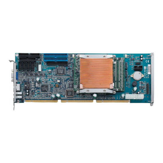
1.4 NuPRO-860 Mechanical Drawing ProCB-860 Carrier Board EM-64 CPU Module Figure 1-1: NuPRO-860 Mechanical Drawing Introduction... -
Page 15: Procb-860 Components And Connectors
1.5 ProCB-860 Components and Connectors 6300ESB GigaLan (82541) FWH (BIOS) Connector to EM-64 (CN21) Primary-IDE (CN16) Secondary-IDE (CN17) CF Interface (CN18) (Secondary-IDE) Super IO (83627HF) LVDS LFP connector (CN20) Ext. Temp Sensor (CN11) DVI connector (CN13) PS/2 KB/MS (CN14) IrDA connector (CN15) COM1~4 (CN5,6,8,10) Parallel port connector (CN7) -
Page 16: Functional Diagram
1.6 EM-64 Functional Diagram Figure 1-3: EM-64 Functional Diagram Introduction... -
Page 17: Unpacking Checklist
1.7 Unpacking Checklist Check the shipping carton for any damage. If the shipping carton and contents are damaged, notify the dealer for a replacement. Retain the shipping carton and packing materials for inspection by the dealer. Obtain authorization before returning any product to ADLINK. - Page 18 Introduction...
-
Page 19: Connectors And Jumpers
Connectors and Jumpers This chapter will familiarize the user with the connectors and jumpers on the NuPRO-860. Please refer to Figure 1-2: ProCB-860 Carrier Board Layout for connector and jumper locations. 2.1 Connector Pin Assignments VGA Connector (CN1) Signal Function Analog RED Green Analog GREEN... -
Page 20: Lan Rj-45 Connector (Cn2))
LAN RJ-45 Connector (CN2)) Signal Function green LAN2_TDP1 Transmit Data1 + LAN2_TDN1 Transmit Data1 - LAN2_RDP2 Receive Data2 + LAN2_RDP3 Receive Data3 + LAN2_RDN3 Receive Data3 - LAN2_RDN2 Receive Data2 - LAN2_TDP4 Transmit Data4 + yellow LAN2_TDN4 Transmit Data4 - LED Color Status Function... -
Page 21: Com 1 - 4 Ports (Cn5, Cn6, Cn8, Cn10)
COM 1 - 4 Ports (CN5, CN6, CN8, CN10) Signal Function Data Carrier Detect Receive Data Transmit Data Data Terminal Ready Ground Data Set Ready Request to Send Clear to Send Ring Indicate No Connect Connectors and Jumpers... -
Page 22: Primary/Secondary Ide Connector (Cn16/Cn17)
Primary/Secondary IDE connector (CN16/CN17) Signal Signal Reset IDE Ground Host data 7 Host data 8 Host data 6 Host data 9 Host data 5 Host data 10 Host data 4 Host data 11 Host data 3 Host data 12 Host data 2 Host data 13 Host data 1 Host data 14... -
Page 23: Atx Power Connector (Cn24)
ATX Power Connector (CN24) Signal Signal +3.3V +3.3V +3.3V -12V PS_ON# PWRGOOD STB5V +12V Connectors and Jumpers... -
Page 24: Floppy Connector (Cn9)
Floppy Connector (CN9) Signal Signal Ground Drive density selection Ground No connect Ground Drive density selection Ground Index Ground Motor enable 0 Ground Drive select 1 Ground Drive select 0 Ground Motor enable 1 Ground Direction Ground Step Ground Write data Ground Write gate Ground... -
Page 25: Front Panel Pin Header (Cn27)
Front Panel Pin Header (CN27) Signal Function Pin Group Power WDTLED# Watchdog LED Signal Power LED Power LED PLED Signal KEYLOCK Keyboard lock Key Lock Ground Ground No connect ATX Power PWRON Power-on signal Connector +5VSB Standby Power Power Management PME# Event WDSPK... -
Page 26: Parallel Port (Cn7)
Parallel Port (CN7) Signal Signal Line printer strobe AutoFeed PD0, parallel data 0 Error PD1, parallel data 1 Initialize PD2, parallel data 2 Select PD3, parallel data 3 Ground PD4, parallel data 4 Ground PD5, parallel data 5 Ground PD6, parallel data 6 Ground PD7, parallel data 7 Ground... -
Page 27: Fan Connectors (Fn1,Fn2)
FAN connectors (FN1,FN2) Signal FAN speed Fan power IrDA Connector (CN15) Signal +3.3V not connected IrRXD Ground IrTXD Connectors and Jumpers... -
Page 28: External Temperature Sensor Connector (Cn11)
External Temperature Sensor Connector (CN11) Signal Function TSEN_I Thermal resistor input TSEN_G Thermal resistor ground External PS/2 KB/MS Connector (CN14) Signal Keyboard data Keyboard clock Mouse data Mouse clock Connectors and Jumpers... -
Page 29: Sata 1, 2 Connectors (Cn22, Cn23)
SATA 1, 2 Connectors (CN22, CN23) Signal AC '97 Interface (CN26)] Signal Signal AC_CLK AC_SDIN0 AC_SDOUT AC_SDIN1 AC_SYNC AC_RSTJ Connectors and Jumpers... -
Page 30: Epci-X Shb Connector Pin Definition
ePCI-X SHB Connector Pin Definition P1 Connector P2 Connector P3 Connector Side B Side A Side B Side A Side B Side A -12V +12V a_AD04 b_VIO b_AD22 PWRGD PWRBT# a_AD05 +3.3V b_C/BE3# PSON# +5Vaux a_AD03 a_AD02 b_AD23 b_AD21 TRST# a_AD00 b_AD20 a_AD01... - Page 31 P1 Connector P2 Connector P3 Connector Side B Side A Side B Side A Side B Side A a_AD26 a_AD37 a_AD36 b_C/BE6# a_C/BE3# a_AD24 a_AD34 b_C/BE5# b_PAR64 a_AD23 +3.3V a_AD35 +3.3V b_C/BE4# +3.3V a_AD22 a_AD33 a_AD32 b_AD62 a_AD21 a_AD20 b_AD63 b_AD60 a_AD19 b_ACLKD...
-
Page 32: Board-To-Board Interface Pin Definition (Cn21)
Board-to-Board Interface Pin Definition (CN21) Segment 1 (Metal Plane: GND) Signal Pin Pin Signal DVOD0 HI_HL10 DVOD1 HI_HL9 DVOD2 VCCP HI_HL8 DVOD3 HI_HL7 DVOD4 Segment 1 DVOD5 HI_HL6 HI_HL5 DVOD6 DVOD7 HI_HL4 DVOD8 HI_HL3 +3.3V DVOD9 HI_HL2 DVOD10 HI_HL1 DVOD11 HI_HL0 DVOCLK HI_STB... - Page 33 IYAP1 IYAM1 CLK33 IYAP0 CLK14 IYAM0 ADDCDATA CLK33_2 Segment 3 (Metal Plane: GND) Signal Pin Pin Signal ADDCCLK PCIRSTJ HIGNNE# HSMI# HNMI HFERR# PWROK_MCH CPUSLP# CPUPWGD DPRSLPVR SMD_SYS DPSLP# SMC_SYS TMDS_I2CC TMDS_I2CD MI2CDATA 101 102 MI2CCLK THERTRIP# 103 104 VRPWRGD 105 106 HINIT# HA20M#...
-
Page 34: Jumper Settings
2.2 Jumper Settings Clear CMOS Jumper (JP1) The ProCB-860 has a clear CMOS jumper on the front of the board to allow the user to clear CMOS values to default values if necessary. To clear the CMOS values, apply a mini jumper to short the pins 2 and 3. -
Page 35: Getting Started
Getting Started This chapter gives a summary of what is required to set up an operating system using the NuPRO-860. Hardware installation and BIOS setup are also discussed. Note that the NuPRO-860 is shipped with CPU, and RAM preinstalled. Installation of the CPU and RAM are performed at the ADLINK factory and the proce- dures described in the following sections are for user reference. -
Page 36: Figure 3-1: Heat Sink Installation
Figure 3-1: Heat Sink Installation Figure 3-2: CPU Installation Getting Started... -
Page 37: Memory Installation
3.2 Memory Installation The NuPRO-860 CPU Module supports 200-pin PC2100/PC2700 registered/unregistered ECC DDR SDRAM up to 2GB maximum. Two memory sockets are located on the CPU Core Module (one on each side). If the required memory modules are pre-installed when the product is received, this section may be skipped. At least one memory module will be installed in the upper DIMM slot of the NuPRO-860 when shipped. -
Page 38: Installing The Second Memory Module
Memory Module Installation). There is an alignment key on the memory module to assist users with installation. Note: Ensure that the CPU socket is in the locked position, otherwise the memory module will not seat properly. Figure 3-3: First Memory Module Installation Installing the second memory module Carefully remove the EM-64 CPU Module from the Carrier Board by removing the mounting screws and lifting it at the end nearest... -
Page 39: Figure 3-4: Em-64 Cpu Module Removal
Figure 3-4: EM-64 CPU Module Removal Figure 3-5: Second Memory Module Installation Getting Started... -
Page 40: Heat Sink Installation
3.3 Heat Sink Installation After you have finished installing the CPU and/or memory mod- ules, replace the heat sink by replacing the four mounting screws. Be sure that the raised blocks on the underside of the heat sink are aligned with the CPU and northbridge on the EM-64 CPU Module (refer to Figure 3-6: Heat Sink Installation below). -
Page 41: Bios Configuration Overview
NuPRO-860. Make sure Pin 1 of the ribbon cable connector is aligned with Pin 1 of the IDE device connector. 3.5 BIOS Configuration Overview This section gives an introduction to the Phoenix/Award Plug and Play BIOS Setup Utility. The BIOS has many separately configurable features. These fea- tures are selected by running the built-in Setup utility. - Page 42 files or documents provided on the distribution disks, as these typ- ically note documentation discrepancies or compatibility problems. Select the appropriate boot device order in the BIOS Setup Utility boot menu depending on the OS installation media used. For example, if the OS includes a bootable installation floppy, select Floppy as the first boot device and reboot the system with the installation floppy installed in the floppy drive.
-
Page 43: Device Driver Installation
Device Driver Installation To install drivers for the NuPRO-850, refer to the installation infor- mation in this chapter. Basic driver installation information for Windows XP/2000 is outlined in this section. The drivers are located in the following directories of the CD-Rom: Chipset driver X:\NuPRO\NuPRO-860\chipset\ VGA driver... -
Page 44: Vga Driver Installation
4. Click Next on the Welcome screen to read and agree to the license agreement. Click Yes if you agree to con- tinue. NOTE: If you click No, the program will terminate. 5. Click Next on the Readme Information screen to install the INF files. -
Page 45: Audio Codec Driver Installation
CD drive letter. For driver installations under other operating sys- tems, please refer to the the ADLINK CD. During Windows 2000/XP installation, the operating system will install a LAN driver automatically. To guarantee compatibility, manually install the most up-to-date driver, which is provided on the ADLINK CD. - Page 46 Device Driver Installation...
-
Page 47: Watchdog Timer
Watchdog Timer The operation of the NuPRO-860’s Watchdog Timer is described in this chapter. An overview of the watchdog operation and fea- tures, as well as the programming procedure is provided to give the user an insight into the workings of the Watchdog Timer. 5.1 WDT Overview The primary function of the Watchdog Timer is to monitor the NuPRO-860’s operation and to generate an IRQ or to reset the... -
Page 48: Configuration Registers
Figure 5-1: WDT Block Diagram 5.2 Configuration Registers The Intel® 6300ESB ICH WDT, appears to BIOS as PCI Bus 0, Device 29, Function 4, and has the standard set of PCI Configura- tion register. The following describes the configuration registers. Offset 10H: Base Address Register (BAR) This register determines the memory base for WDT down- counter setting. - Page 49 The register unlocking sequence is necessary whenever writ- ing to the Preload registers. Instructions for writing a value into preload value 1 & 2 registers are as follows: 1. Write 80H to offset BAR + 0CH. 2. Write 86H to offset BAR + 0CH. 3.
-
Page 50: Wdt Programming Procedure
Offset 68H: WDT Lock Register Bit 2 is used to choose the functionality of the timer. (0 = Watchdog Timer mode, 1 = Free running mode) The free-run- ning mode ignores the first stage and only uses Preload Value 2. In free-running mode it is not necessary to reload the timer as it is done automatically every time the down-counter reaches zero. -
Page 51: Epci-X Bus Details
ePCI-X Bus Details 6.1 NuPRO-860 ePCI-X Bus The NuPRO-860 provides both PCI-X and PCI buses. Bus-A sup- ports 64-bit /66MHz PCI-X and bus-B supports 32-bit/33MHz PCI. The ePCI-X Bus pin assignment is compatible with the PICMG 1.2 ePCI-X specification. In the following sections, we will describe the detailed signal definitions of the NuPRO-860 ePCI-X bus to assist in backplane selection and design. -
Page 52: Pci-X Bus Signals
6.3 PCI-X Bus Signals Backplane Present The a_PRSNT# and b_PRSNT# signals are connected to the Super I/O chip’s GP25 and GP26 pins respectively. These sig- nal are pulled to +3.3V via 4.7k resistors. VIO Electrical Keying The NuPRO-860 monitors the VIO keying signals from the backplane. -
Page 53: Warranty Policy
Warranty Policy Thank you for choosing ADLINK. To understand your rights and enjoy all the after-sales services we offer, please read the follow- ing carefully. 1. Before using ADLINK’s products please read the user man- ual and follow the instructions exactly. When sending in damaged products for repair, please attach an RMA appli- cation form which can be downloaded from: http:// rma.adlinktech.com/policy/. - Page 54 3. Our repair service is not covered by ADLINK's guarantee in the following situations: Damage caused by not following instructions in the User's Manual. Damage caused by carelessness on the user's part dur- ing product transportation. Damage caused by fire, earthquakes, floods, lightening, pollution, other acts of God, and/or incorrect usage of voltage transformers.
Need help?
Do you have a question about the NuPRO-860 Series and is the answer not in the manual?
Questions and answers