Table of Contents
Advertisement
Quick Links
Advertisement
Table of Contents

Related Manuals for ADLINK Technology CM1-86DX3


Summary of Contents for ADLINK Technology CM1-86DX3
- Page 1 CM1-86DX3 Technical Reference PC/104 Single Board Computer with Vortex86-DX3 SoC Manual Rev.: Revision Date: February 4, 2021 Part Number: 50-1Z161-1070 Manual Rev.: Revision Date: February 4, 2021 Part Number: 50-1Z174-1050 Leading EDGE COMPUTING...
-
Page 2: Preface
Add French safety warnings 2021-02-04 Copyright © 2015, 2016, 2017, 2018, 2020, 2021 ADLINK Technology, Inc. This document contains proprietary information protected by copyright. All rights are reserved. No part of this manual may be reproduced by any mechanical, electronic, or other means in any form without prior written permission of the manufacturer. - Page 3 CM1-86DX3 Environmental Responsibility ADLINK is committed to fulfill its social responsibility to global environmen- tal preservation through compliance with the European Union's Restriction of Hazardous Substances (RoHS) directive and Waste Electrical and Elec- tronic Equipment (WEEE) directive. Environmental protection is a top prior- ity for ADLINK.
- Page 4 Conventions The following conventions may be used throughout this manual, denoting special levels of information. This information adds clarity or specifics to text and illustrations. This information indicates the possibility of minor physical injury, component damage, data loss, and/or program corruption. Ces informations indiquent la possibilité...
-
Page 5: Table Of Contents
CM1-86DX3 Table of Contents Preface ........................... ii 1 Product Overview......................1 Description..........................1 About this Manual ........................1 Features..........................2 Ordering Information....................... 2 Block Diagram ........................3 Specifications..........................4 1.6.1 Physical ......................... 4 1.6.2 Mechanical ........................4 1.6.3 Electrical ......................... 5 1.6.4 Power .......................... - Page 6 3.11 Power Button Interface......................31 3.12 CFast Mass Storage Socket....................31 4 Utilities ..........................33 BIOS Setup .......................... 33 4.1.1 Configuring the BIOS ....................33 4.1.2 Main screen of the BIOS ....................33 4.1.3 Advanced Settings screen ................... 34 4.1.4 Boot screen ........................
-
Page 7: Product Overview
System expansion is provided over the PC/104 connector. The CM1-86DX3 is powered by a 5V-only supply and runs DOS, Windows XP/7 and Linux oper- ating systems. The Vortex86-DX3 SoC has a simulated ACPI to support Windows 7 (though S3 or S4 modes are not supported.) -
Page 8: Features
PC/104 with Vortex 86DX3, 2GB soldered DDR3, 10/100 Ethernet, CM1-86DX3 GbE, CFast socket, TTL LCD and VGA display Table 1-2: Cable Sets and Accessories Model Number Description Adapter Cable Set CM1-86DX3-X-01 CM1-86DX3-TM-20 passive heatsink for -40°C to +85°C operating CM1-86DX3-TM-20 range, with airflow requirements Product Overview... -
Page 9: Block Diagram
CM1-86DX3 Block Diagram Figure 1-1 provides a functional representation of the CM1-86DX3. CM1-86DX3 2GB DDR3-800/1333 DDR3 – 1.5V Level Shifter 18/24-bit Memory Down TTL/TFT Backlight SATA SATA VGA-DDC CFast i210IT SMBus PCIe 8x GPIO PCA9535BS Vortex86DX3 Ethernet KB, Mouse, Speaker, RESET... -
Page 10: Specifications
Specifications 1.6.1 Physical Table 1-3 provides the physical dimensions of the module. Table 1-3: Weight and Footprint Dimensions Overall height is measured from the upper board Item Dimension surface to the highest permanent component (PC/ Weight 0.12 kg (0.25 lbs) 104 bus connector) on the upper board surface. -
Page 11: Electrical
S3, S4, S5 (S3 and S4 not supported by Win- dows 7) Power Management ACPI compliant 1.6.4 Power Table 1-5 provides the power consumption values of the CM1-86DX3. Table 1-5: Power Supply Requirements Parameter Board Characteristics Input Type Regulated DC voltage Typical Idle Current and Power 1.04A (5.20W) -
Page 12: Thermal/Cooling Requirements
1.6.6 Thermal/Cooling Requirements The CM1-86DX3 is designed to operate at its maximum CPU speed and requires a thermal solution to cool the CPU. ADLINK offers a heat spreader and a passive heatsink (separate order numbers) for cooling. The heatsink can be used for module evaluation. If a custom heatsink is used, it is recommended to connect it to the ADLINK heat spreader. - Page 13 Figure 1-5 presents four separate directions of airflow across the fins of the passive heatsink. Refer to Figure 1-4 for required airflow ratios with regard to each of the airflow directions. Airflow Direction 4 Airflow Airflow Direction 1 Direction 2 Airflow Direction 3 Figure 1-5: Airflow Directions with CM1-86DX3-TM Heatsink Product Overview...
-
Page 14: Heat Sink Installation
Heat Sink Installation Follow the steps below to mount the passive heat sink to the top side of the board. The heat sink features thermal pads to draw heat away from the SoC, SDRAM, BMC controller, and other transceivers. 1. Locate the heat sink kit in the package. The thermal pads are labelled with their corre- sponding parts on the board 2. - Page 15 CM1-86DX3 3. Align the heat sink with the board as shown below. The five mounting holes on the board are circled in red. 4. Place the heat sink over the board so that the five mounting holes on the heat sink are aligned with mounting holes on the board.
- Page 16 6. Turn the board and heat sink assembly over and secure the heat sink to the board with five M2.5 screws (torque: 2 kgf.cm) as shown below. 7. The heat sink installation is now complete. Product Overview...
-
Page 17: Getting Started
MISE EN GARDE Use the cable set provided by ADLINK Technology to connect the CM1-86DX3 to a VGA moni- tor. Connect either PS/2 or USB keyboard or mouse, respectively. Use the SATA cable to con- nect the hard disk. - Page 18 This page intentionally left blank. Product Overview...
-
Page 19: Hardware
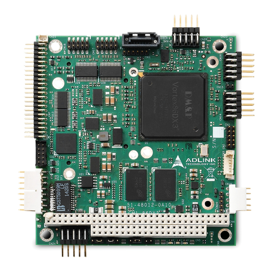
Major IC Definitions and Locations Table 2-1 describes the major ICs on the CM1-86DX3, including a brief description of each IC. Figures 2-1 and 2-2 show the locations of the major ICs. Table 2-1: Major Component Descriptions and Functions Chip Type Mfg. - Page 20 Table 2-1: Major Component Descriptions and Functions (Continued) Chip Type Mfg. Model Description Function BMC (U33) Texas TM4C123BH6ZRBIR Microcontroller Provides [Optional] Instruments logistics and forensic information, flat panel control, I2C bus control, user flash, Watchdog Timer and fan control Gb Ethernet BOTHHAND GST5009M Gigabit Ethernet...
- Page 21 CM1-86DX3 Key: - DDR3 SDRAM - System Memory U10 - DDR3 SDRAM - System Memory U22 - Controller - 10/100/1000 Gb Ethernet U26 - Transceiver - COM1 RS-485/422/232 U27 - Transceiver - COM2 RS-485/422/232 TF2 - Transformer - 10/100/1000 Gb Ethernet...
-
Page 22: Header, Connector, And Socket Definitions
Header, Connector, and Socket Definitions Table 2-2 describes the headers, connectors, and sockets shown in Figures 2-3 and 2-4. Table 2-2: Header, Connector, and Socket Descriptions Jack/Plug # Access Description CN2 – GPIO (User) 10-pin, 0.079" (2mm) header for User defined GPIO signals [TEKA, HM205CB1N-191-00] CN3 –... - Page 23 CM1-86DX3 Table 2-2: Header, Connector, and Socket Descriptions (Continued) Jack/Plug # Access Description CN24 – Power 10-pin, 0.100" (2.54mm), right-angle header for Power connection [TEKA, HR205A1BB-NS-H0] CN25 – Battery 2-pin, 0.049" (1.25mm) header for external battery [REGO, 830-1251-02STD-3.2-6T] CN26 – Utility 10-pin, 0.100"...
- Page 24 Key: CN13 - CFast CN22 - Debug - DB40 - PC/104 (A/B) - PC/104 (C/D) LED3 - CFAST_ACT LED3 CN22 CN13 Figure 2-4: Header and Socket Locations (Bottom Side) Pin 1 is shown as a solid, black square on headers and connectors.
-
Page 25: Jumper Header Definitions
CM1-86DX3 Jumper Header Definitions Table 2-3 describes the jumper headers shown in Figure 2-5. All jumper headers provide 0.079" (2mm) pitch. Table 2-3: Jumper Settings Jumper Header Jumper on Pins 1-2 Jumper on Pins 2-3 JP1 – TFT Interface Voltage +1.8 Volts... -
Page 26: Component Features
Component Features This section further describes the supported features of the CM1-86DX3 major, on-board hard- ware components. 2.4.1 The CM1-86DX3 features the DMP Electronics Vortex, VX86DX3 CPU, System-on-Chip (SoC). The VX86DX3 is a high-performance and fully static, 32-bit x86 processor with the compatibility of Windows-based, Linux, and most popular 32-bit RTOS. -
Page 27: Cfast Card Slot
CM1-86DX3 2.4.3 CFast Card Slot The CFast slot (CN13) provides the standard, push-push interface for CFast memory cards. LED3 provides indication of CFast activity. See Chapter 3 for the signal definitions of the CFast interface. Figure 2-6 provides the dimension and mechanical specifications of the CFast card connector. - Page 28 This page intentionally left blank. Hardware...
-
Page 29: Interfaces
CM1-86DX3 Interfaces This chapter provides descriptions and signal definitions only of the non-standard interfaces on the board. Descriptions and signal definitions of standard interfaces such as PC/104 and SATA can be found in their respective specification data sheets. If certain signals of standard inter- faces have been modified or disconnected, those interfaces will be described in this chapter. - Page 30 Table 3-1: Serial Port 1 (CN16) & Port 2 (CN14) Interface Pin Signals Pin # Signal DB9 # Description DCD* Data Carrier Detect – Indicates external serial device is detecting a carrier signal (i.e., a communication channel is currently open). In direct connect environments, this input is driven by DTR as part of the DTR/DSR handshake.
- Page 31 CM1-86DX3 Table 3-2: Serial Port 3 (CN17) & Port 4 (CN18) Interface Pin Signals Pin # Signal DB9 # Description DCD* Data Carrier Detect – Indicates external serial device is detecting a carrier signal (i.e., a communication channel is currently open). In direct connect environments, this input is driven by DTR as part of the DTR/DSR handshake.
-
Page 32: Usb Interfaces
USB Interfaces The CM1-86DX3 provides one root USB hub and two functional USB ports, supporting USB EHCI v2.0 and over-current detection. Table 3-3 describes the pin signals of the USB0 interface, which uses a single-row, 5-pin, right-angle header with 0.100" (2.54mm) pitch. -
Page 33: Reset Switch
CM1-86DX3 3.3.4 Reset Switch An external reset switch provides the reset signal through the Utility interface to a reset circuit, which drives the Vortex CPU. 3.3.5 Speaker Ω The speaker signal provides sufficient signal strength to drive a 1W 8 “Beep”... -
Page 34: Gigabit Ethernet Interface
Gigabit Ethernet Interface Table 3-7 describes the pin signals of the Gigabit Ethernet header which consists of 10 right-angle pins, two rows, odd/even (1,2) pin sequence, and 0.079" (2mm) pitch. Table 3-7: Gigabit Ethernet Interface Pin Signals (CN9) Pin # Signal Description ETH-PE... - Page 35 CM1-86DX3 Table 3-9: Video Interface Pin Signals (CN7) (Continued) Pin # Signal Description Flat Panel Data 3 – data output, Blue1 (18-bit) Flat Panel Data 4 – data output, Blue2 (18-bit) Flat Panel Data 5 – data output, Blue3 (18-bit) Flat Panel Data 6 –...
-
Page 36: Vga Ddc (Display Data Channel)
Display Data Channel data Power Interface The CM1-86DX3 requires one +5 volt DC power source. If the +5VDC power drops below ~4.65V, a low voltage reset is triggered, resetting the system. The power input header (CN24) supplies the following voltages and ground directly to the mod- ule: 5.0VDC +/- 5% @ 1.35 Amps... -
Page 37: Power Button Interface
CM1-86DX3 3.11 Power Button Interface Table 3-13 lists the pin signals of the External Power Button header, which uses 2 pins with pitch. 0.079" (2mm) Table 3-13: External Power Button Header (CN27) Pin # Signal Description PWRBTN# +3.3 volts for power button Ground Note: The shaded table cells denote power or ground. - Page 38 This page intentionally left blank. Interfaces...
-
Page 39: Utilities
Utilities BIOS Setup The CM1-86DX3 features an AMI BIOS. The default settings provide a “ready to run” system, even without a BIOS setup backup battery. The BIOS is located in flash memory and can be easily updated with software under DOS. -
Page 40: Advanced Settings Screen
4.1.3 Advanced Settings screen The main screen of “Advanced Settings” provides configuration settings for the IDE interface, serial port, remote access, and USB port. Refer to the following illustrations for visual reference. A description of the selected setting appears in the right column of the active screen. The use of inappropriate values on any of the following advanced settings below may cause the system to malfunction. - Page 41 CM1-86DX3 Advanced > IDE Configuration These settings allow you to configure the features of the integrated IDE controllers. Advanced > IDE Master This setting provides options for IDE slave and master drives. Utilities...
- Page 42 Advanced > Serial Port These settings allow you to specify the base I/O port address, Interrupt Request address, and Port Type mode (if applicable) of specific serial ports. Advanced > Remote Access Remote Access allows you to enter the BIOS Setup through a serial terminal or PC. Utilities...
-
Page 43: Boot Screen
USB drivers are loaded on the system. 4.1.4 Boot screen If more than one drive is attached to the CM1-86DX3, you can select from the first “Boot Set- tings” screen the boot order in which the drives are scanned for a bootable OS image. Boot Settings The Boot From LAN setting allows you to enable LAN PXE boot. -
Page 44: Security Screen
Boot > Boot Device Priority These settings allow you to specify the order in which the system checks for the device from which to boot. 4.1.5 Security screen This screen allows you to set a Supervisor or a User password. If you want to use both pass- words, the Supervisor password must be set first. -
Page 45: Exit Screen
CM1-86DX3 4.1.6 Exit screen The settings in the Exit screen allow you to exit the BIOS Setup utility while saving or discarding certain defaults or changes. Utilities... -
Page 46: Sema Functions
SEMA Functions Under the management of the BMC chip (Board Management Controller), the SEMA utility (Smart Embedded Management Agent) provides system control and failure protection—count- ing, monitoring, and measuring hardware and software events, from which the SoC can trigger corrective commands. The optional SEMA Cloud utility not only controls local events on the module but system client events on the Internet of Things (IoT.) Refer to the following bullets for a list of SEMA functions. -
Page 47: Board Specific Sema Functions
Use Main Current Function Main Current The BMC of the CM1-86DX3 implements a Current Monitor. The current can be read by call- ing the SEMA function “Get Main Current”. The function returns four 16-bit values divided in Hi-Byte (MSB) and Lo-Byte (LSB). These four values represent the last four currents drawn by the board. -
Page 48: Real Time Clock (Rtc)
The BMC Flags register returns the last detected exception code since power up. Real Time Clock (RTC) The CM1-86DX3 contains a Real Time (time of day) Clock (RTC), which can be backed up with an external Lithium Battery. The CM1-86DX3 will function without a battery in those environ- ments which prohibit batteries. -
Page 49: User Gpio Interface
(CN14 or CN16) to the serial terminal or a PC with communications software. The BIOS Setup Utility controls the serial console settings on the CM1-86DX3. Refer to the BIOS Setup for the serial console option settings using a serial terminal or PC with communications software. -
Page 50: Hot (Serial) Cable
Watchdog Code examples – ADLINK has provided source code examples in the CM1-86DX3 SEMA, illustrating how to control the WDT. The code examples can be easily copied to your environment to compile and test, or to make any desired changes before compiling. -
Page 51: Appendix A System Resources
CM1-86DX3 Appendix A System Resources This appendix provides system resource specifications for the CM1-86DX3 including Memory addresses, IO addresses, PCI configuration registers, IO registers, and system interrupts. A.1 Memory Address Map The SoC supports 4 GBytes of addressable memory space and 64 KBytes of addressable I/O space. - Page 52 System BIOS Area (F0000–FFFFFh) This area is a single 64-KByte segment that can be assigned read and write attributes. It is by default (after reset) read/write disabled and cycles are forwarded to the PCI bus. By manipulat- ing the read/write attributes, the SoC can “shadow” BIOS into main memory. Memory that is dis- abled is not remapped.
-
Page 53: I/O Address Map
CM1-86DX3 A.2 I/O Address Map The SoC positively decodes accesses to all internal registers, including PCI configuration regis- ters (CF8h and CFCh), PC/AT Compatible IO registers (8237, 8254 & 8259), and all re-locatable IO space registers (UART). Table A-1: Fixed IO Ranges in the CPU... - Page 54 Table A-2: Variable IO Address Ranges Decoded by PCI Devices in the IO Fabric Device Size / Bytes Comment ACPI Power Management ACPI BASE ADDRESS: (PCU) PCI[B:0,D:7,F:0] + F8h I2C BASE ADDRESS: PCI[B:0,D:7,F:0] + D4h Variable IO ranges should not be set to conflict with other IO ranges. There will be unpredictable results if the configuration software allows conflicts to occur.
-
Page 55: Pci Configuration Registers
CM1-86DX3 A.3 PCI Configuration Registers Devices and functions can be accessed by the PCI Configuration Registers. Table A-3: PCI Configuration Registers Address Range (hex) Description 0CFB – 0CF8 PCI Configuration Address Register 0CFF – 0CFC PCI Configuration Data Register Table A-4: PCI CONFIG_ADDRESS Register Mapping (IO Port CF8h) -
Page 56: Io Register Maps
A.4 IO Register Maps A.4.1 CMOS Memory and RTC Registers The RTC internal registers and RAM are organized as two banks of 128 bytes each, called the standard and extended banks. The first 14 bytes of the standard bank contain the RTC time and date information along with four registers A-D, that are used for configuration of the RTC. -
Page 57: Interrupts
CM1-86DX3 A.5 Interrupts A.5.1 SERIRQ Interrupt Mapping Below the SERIRQ Interrupt Mapping is shown: Table A-8: SERRIRQ Interrupt Mapping Data Interrupt Comment Frame# IRQ0 System Timer IRQ1 Keyboard Controller IRQ2 Cascade for IRQ8~15 IRQ3 Serial port 2 IRQ4 Serial port 1... - Page 58 This page intentionally left blank.
-
Page 59: Appendix B Technical Support
San Jose, CA 95138, USA Tel: +1-408-360-0200 Toll Free: +1-800-966-5200 (USA only) Fax: +1-408-360-0222 Email: info@adlinktech.com ADLINK Technology (China) Co., Ltd. 300 Fang Chun Rd., Zhangjiang Hi-Tech Park Pudong New Area, Shanghai, 201203 China Tel: +86-21-5132-8988 Fax: +86-21-5132-3588 Email: market@adlinktech.com...
Need help?
Do you have a question about the CM1-86DX3 and is the answer not in the manual?
Questions and answers