Table of Contents
Advertisement
Quick Links
Advertisement
Table of Contents

Related Manuals for Humandata Spartan-3


Summary of Contents for Humandata Spartan-3
- Page 1 Spartan-3 FPGA Board XCM-005 Series User’s Manual HuMANDATA LTD.
-
Page 2: Table Of Contents
Table of Contents Revision History ....................1 Introduction......................1 1. Specifications......................2 2. Overview........................ 3 2.1. Name of Parts ....................3 2.2. Block Diagram ....................4 2.3. Power Supply ..................... 4 2.4. JTAG Connector....................5 3. Jumper Pins......................5 3.1. Configuration Pin ....................5 4. - Page 3 HuMANDATA will revise the diagram. When a problem can be solved only by replacing components or modifying the product, HuMANDATA will take back the product to replace it with a properly functioning product.
-
Page 4: Revision History
Initial release Introduction Thank you for buying our product XCM-005. This is an evaluation board equipped with a Xilinx FPGA Spartan-3, power, reset, and clock circuit and configuration device. It can provide you with very convenient and easy-to-use environment. XCM-005 Series v1.0... -
Page 5: Specifications
1. Specifications Model Name XCM-005-1000 XCM-005-1500 XCM-005-2000 FPGA XC3S1000-4FGG456C XC3S1500-4FGG456C XC3S2000-4FGG456C Configuration Device XCF04S (Xilinx) XCF04S x 2 SDRAM MT48LC16M16A2P-75-D (MICRON, 256 Mbit) User I/Os On-Board Clock 48 [MHz], 18.432 [MHz] (External inputs are available) Status LEDs 2 (POWER, DONE) Power-On Reset 200 [ms] typ. -
Page 6: Overview
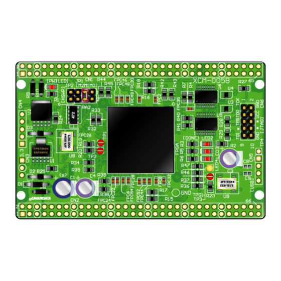
2. Overview 2.1. Name of Parts User I/Os (CN1) JTAG Power & POR Config. Device FPGA Oscillator 48 MHz Oscillator 18.432 MHz User I/Os (CN2) Component Side *XCM-005-1500/2000 XCM-005 Series v1.0... -
Page 7: Block Diagram
3.3 V INPUT External CLK User I/Os CNB Config. Jumper Oscillator 18.432 MHz Config. Device XCF04S (4 Mbit) SDRAM (256 Mbit) (1500/2000 only) Spartan-3 PROG_B Config. Device XC3S1000/1500/2000 RESET XCF04S -4FGG456C (4 Mbit) POR Signal Power Circuit 2.5V, 1.2V JTAG... -
Page 8: Jtag Connector
2.4. JTAG Connector This connector is used to configure the FPGA and program the configuration device in-system. Pin assignment is as follows. Signal Name JTAG Pin Signal Name VCC (3.3V) You can use Xilinx download cable. Notice Please pay attention not to attach cables in reverse. 3. -
Page 9: Fpga Configuration
4. FPGA Configuration To configure the FPGA via JTAG, please refer to the following steps. 1. Double-click [Configuration Target Device] in [Processes] tab. 2. Select [Configure devices using Boundary-Scan (JTAG)]. 3. Open the bit file you made. 4. Confirm [Verify] is not checked in [Device Programming Properties] dialog. 5. -
Page 10: Additional Documentation And User Support
6. Additional Documentation and User Support The following documents and other supports are available at http://www.hdl.co.jp/en/spc/XCM/xcm-005/ Circuit Schematic Pin List Dimensional drawing PCB drawing Net List … and more. XCM-005 Series v1.0... - Page 11 Spartan-3 FPGA Board XCM-005 Series User’s Manual Ver. 1.0 ..........Jul. 15, 2009 HuMANDATA LTD. Address: 1-2-10-2F, Nakahozumi, Ibaraki Osaka, Japan ZIP 567-0034 Tel: 81-(0)72-620-2002 (Japanese) Fax: 81-(0)72-620-2003 (Japanese/English) URL: http://www.hdl.co.jp/en/ (Global) http://www.hdl.co.jp/ (Japan)
Need help?
Do you have a question about the Spartan-3 and is the answer not in the manual?
Questions and answers