Table of Contents
Advertisement
Quick Links
Advertisement
Table of Contents

Related Manuals for Humandata XCM-110Z Series


Summary of Contents for Humandata XCM-110Z Series
- Page 1 Spartan-6 FPGA Board XCM-110Z Series User’s Manual Ver. 1.1 HuMANDATA LTD.
-
Page 2: Table Of Contents
Table of Contents Revision History ....................1 Introduction ....................1 1. Shared Pins [IMPORTANT] ................2 2. Specifications ..................... 3 3. Overview ......................4 3.1. Name of Parts .......................4 3.2. Block Diagram ......................5 3.3. Power Supply ......................5 3.4. Clock ........................6 3.5. - Page 3 HuMANDATA will revise the diagram. When a problem can be solved only by replacing components or modifying the product, HuMANDATA will take back the product to replace it with a properly functioning product.
-
Page 4: Revision History
This is an evaluation board equipped with a Xilinx FPGA Spartan-6, voltage regulators, configuration reset circuit, oscillators and configuration device. XCM-110Z series are derived from XCM-110 series by removing MRAM and DDR2 SDRAM. It can provide you with very convenient and easy-to-use development environment. -
Page 5: Shared Pins [Important]
To prevent these pins from being shorted out, it is recommended to set them as “Float” in advance. Please refer to the following steps and check the “Unused IOB Pins” setting. 1. Right click [Generate Programming File] and open [Process Properties] window. 2. Confirm [Unused IOB Pins] in [Configuration Options]. XCM-110Z Series v1.1... -
Page 6: Specifications
SIL 7-pin socket, 2.54 [mm] pitch Status LEDs Power (red) x1, Done (blue) x1 SIL 7-pin header (Mounted) x1 Accessories FX10A-80S/8-SV(71) (Hirose) x 2 RoHS Compliance * There may be cases that these parts and specifications are changed. XCM-110Z Series v1.1... -
Page 7: Overview
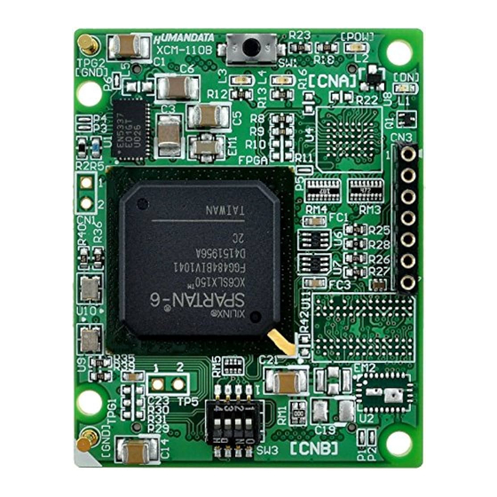
3. Overview 3.1. Name of Parts User Switch POWER LED User LEDs DONE LED Oscillator 30 MHz Oscillator 50 MHz JTAG Config. Switch Component Side User I/Os (CNA) Config. Device User I/Os (CNB) Solder Side XCM-110Z Series v1.1... -
Page 8: Block Diagram
The external power supply should be sufficient and stabilized. Please do not apply over 3.3V voltage. VCCIO in BANK B is not connected to 3.3V. Please input given voltage from CNB. For more details, please refer to circuit schematics and FPGA data sheet. XCM-110Z Series v1.1... -
Page 9: Clock
JTAG connector is used to configure the FPGA and program the configuration device in-system. Pin assignment is as follows. You can use Xilinx download cable. Pin No. Signal Name Direction OUT (POW) Notice Please pay attention not to attach cables in reverse. XCM-110Z Series v1.1... -
Page 10: Configuration Switch (Sw3)
User I/O pull-up control. When low during configuration, enables pull-up resistors in all I/O pins to respective I/O bank VCCO input. ON : Pull-ups during configuration OFF : No Pull-ups For more detail, please refer to Xilinx Spartan-6 data sheet. XCM-110Z Series v1.1... -
Page 11: Fpga Configuration
Assign the mcs file to a Flash icon and choose [SPI PROM – M25P32] or [SPI PROM – M25P64] for device type, then right click and select a command. Please set FPGA configuration mode to [Master Serial/SPI] mode. XCM-110Z Series v1.1... -
Page 12: Additional Documentation And User Support
6. Additional Documentation and User Support The following documents and other supports are available at http://www.hdl.co.jp/en/spc/XCM/xcm-110Z/ Circuit Schematic Pin List Dimensional drawing Net List … and more. XCM-110Z Series v1.1... - Page 13 Spartan -6 FPGA Board XCM-110Z Series User’s Manual Ver. 1.1 ..........Dec. 11, 2013 HuMANDATA LTD. Address: 1-2-10-2F, Nakahozumi, Ibaraki Osaka, Japan ZIP 567-0034 Tel: 81-72-620-2002 (Japanese) Fax: 81-72-620-2003 (Japanese/English) URL: http://www.hdl.co.jp/en/ (Global) http://www.hdl.co.jp/ (Japan)
Need help?
Do you have a question about the XCM-110Z Series and is the answer not in the manual?
Questions and answers