Table of Contents
Advertisement
Quick Links
Advertisement
Table of Contents

Related Manuals for Humandata XCM-206Z


Summary of Contents for Humandata XCM-206Z
- Page 1 Spartan-6 FPGA Board XCM-206Z Series User’s Manual Ver. 2.2 HuMANDATA LTD.
-
Page 2: Table Of Contents
Table of Contents Revision History ....................1 Introduction ....................1 1. Share Pins [IMPORTANT] ................. 2 2. Specifications ..................... 4 3. Overview ......................5 3.1. Name of Parts .......................5 3.2. Block Diagram ......................6 3.3. Power Supply ......................7 3.4. Clock ........................7 3.5. - Page 3 HuMANDATA will revise the diagram. When a problem can be solved only by replacing components or modifying the product, HuMANDATA will take back the product to replace it with a properly functioning product.
-
Page 4: Revision History
Typo fix: JTAG connector table Introduction Thank you for buying our product XCM-206Z. This is an evaluation board equipped with a Xilinx FPGA Spartan-6, voltage regulators, configuration reset circuit, oscillators and configuration device. It can provide you with very convenient and easy-to-use development environment. -
Page 5: [Important]
For LX75 device, they are connected but Bank group B I/Os are NC pins. LX100/150 Connection LX75 Connection IOB46 IOB47 IOB48 IOB49 IOB50 IOB51 IOB52 IOB53 IOB54 IOB55 IOB56 IOB57 IOB58 IOB59 IOB60 IOB61 IOB62 IOB63 Bank Group B Bank Group A Bank Group B Bank Group A XCM-206Z Series v2.2... - Page 6 To prevent these pins from being shorted out, it is recommended to set them as “Float” in advance. Please refer to the following steps and check the “Unused IOB Pins” setting. 1. Right click [Generate Programming File] and open [Process Properties] window. 2. Confirm [Unused IOB Pins] in [Configuration Options]. XCM-206Z Series v2.2...
-
Page 7: Specifications
SIL 7-pin socket, 2.54 [mm] pitch Status LEDs Power (red) x1, Done (blue) x1 SIL 7-pin header (Mounted) x1 FX10A-80S/8-SV(71) x2 Accessories FX10A-100S/10-SV(71) x2 (Hirose Electric) Spacer x4 RoHS Compliance * There may be cases that these parts and specifications are changed. XCM-206Z Series v2.2... -
Page 8: Overview
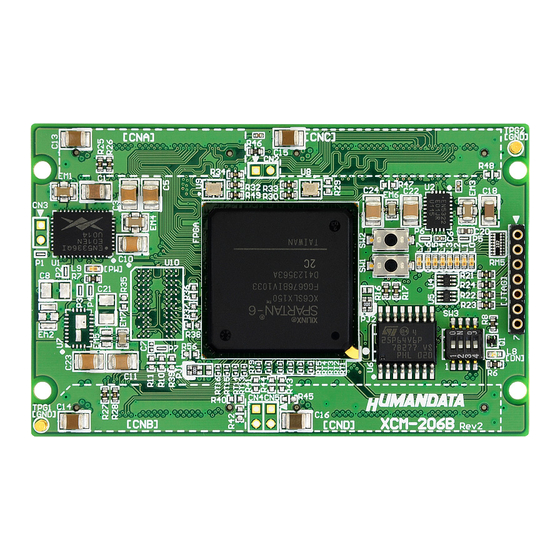
3.1. Name of Parts Oscillator 50 MHz Oscillator 30 MHz User Switches User LEDs JTAG Power LED Config. SW DONE LED Config. Device Component Side User I/Os (CNA) User I/Os (CNC) User I/Os (CNB) User I/Os (CND) Solder Side XCM-206Z Series v2.2... -
Page 9: Block Diagram
B uffer Power Circuit 2 .5V,1.2V C onfig. Switch Power LED (3.3V) 148 GPIO U s er I/Os CNB U s er I/Os CND V IO(B) INPUT E xt . Clock (Option) V IO(D) INPUT X CM-206Z Rev.D XCM-206Z Series v2.2... -
Page 10: Power Supply
This connector is used to configure the FPGA and program the configuration device in-system. Pin assignment is as follows. You can use Xilinx download cable. Direction Pin No. Signal Name OUT (POW) Notice Please pay attention not to attach cables in reverse. XCM-206Z Series v2.2... -
Page 11: Configuration Switch (Sw3)
Generally, users do not need to be attentive to mode setting for JTAG configuration. But for this product, it is recommended to set the mode as shown above. ASW0, ASW1 You can use this as user switch. XCM-206Z Series v2.2... -
Page 12: Fpga Configuration
Select your bit file, and generate MCS file. 5.2. Programming Configuration Device Assign the mcs file to Flash icon and choose [SPI PROM – M25P64] for device type, then right click and select a command. Please set FPGA configuration mode to [Master Serial/SPI] mode. XCM-206Z Series v2.2... -
Page 13: Additional Documentation And User Support
6. Additional Documentation and User Support The following documents and other supports are available at http://www.hdl.co.jp/en/spc/XCM/xcm-206Z/ Circuit Schematic Pin List Dimensional drawing Net List … and more. XCM-206Z Series v2.2... - Page 14 Spartan -6 FPGA Board XCM-206Z Series User’s Manual Ver. 2.2 ..........Jul. 25, 2012 HuMANDATA LTD. Address: 1-2-10-2F, Nakahozumi, Ibaraki Osaka, Japan ZIP 567-0034 Tel: 81-72-620-2002 (Japanese) Fax: 81-72-620-2003 (Japanese/English) URL: http://www.hdl.co.jp/en/ (Global) http://www.hdl.co.jp/ (Japan)
Need help?
Do you have a question about the XCM-206Z and is the answer not in the manual?
Questions and answers