Table of Contents
Advertisement
Quick Links
Advertisement
Table of Contents

Related Manuals for Humandata XCM-111


Summary of Contents for Humandata XCM-111
- Page 1 Spartan-6 LXT FPGA Board XCM-111 Series User’s Manual Ver. 1.0 HuMANDATA LTD.
-
Page 2: Table Of Contents
Table of Contents Revision History ....................1 Introduction ......................1 1. Shared Pins [IMPORTANT] .................. 2 2. Specifications ......................3 3. Overview ........................ 4 3.1. Name of Parts ....................4 3.2. Block Diagram ....................5 3.3. Power Supply ..................... 5 3.4. - Page 3 HuMANDATA will revise the diagram. When a problem can be solved only by replacing components or modifying the product, HuMANDATA will take back the product to replace it with a properly functioning product.
-
Page 4: Revision History
Initial release Introduction Thank you for buying our product XCM-111. This is an evaluation board equipped with a Xilinx FPGA Spartan-6 LXT series, voltage regulators, configuration reset circuit, oscillators and configuration device. It can provide you with very convenient and easy-to-use development environment. -
Page 5: Shared Pins [Important]
To prevent these pins from being shorted out, it is recommended to set them as “Float” in advance. Please refer to the following steps and check the “Unused IOB Pins” setting. 1. Right click [Generate Programming File] and open [Process Properties] window. 2. Confirm [Unused IOB Pins] in [Configuration Options]. XCM-111 Series v1.0... -
Page 6: Specifications
1.693" x 2.126" (43 x 54 [mm]) Weight 20 [g] typ. User I/O Connectors FX10A-80P/8-SV1(71) (Hirose) x 2 SIL7 long pin header (Mounted) x1 Accessories FX10A-80S/8-SV(71) (Hirose) x 2 RoHS Compliance * There may be cases that these parts and specifications are changed. XCM-111 Series v1.0... -
Page 7: Overview
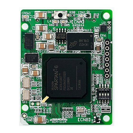
3. Overview 3.1. Name of Parts Done LED Power LED User Switch DDR2 SDRAM User LEDs JTAG FPGA Config. Switch RocketIO Ref. Clock User Switch Oscillator Component Side User I/Os (CNA) Config. Device User I/Os (CNB) Solder Side XCM-111 Series v1.0... -
Page 8: Block Diagram
You can use user Vcco for CNB I/Os. The Vcco, VIO(B), is not connected to the V33A. Please input arbitrary voltage into it. On-board 2.5V can be applied by setting the zero ohm resister (PJ1). For more details, please refer to circuit schematics and FPGA data sheet. XCM-111 Series v1.0... -
Page 9: Clock
JTAG connector is used to configure the FPGA and program the configuration device in-system. Pin assignment is as follows. You can use Xilinx download cable. Pin No. Signal Name Direction VCC (3.3V) OUT (POW) Notice Please pay attention not to attach cables in reverse. XCM-111 Series v1.0... -
Page 10: Configuration Switch (Sw1)
Generally, users do not need to be attentive to mode setting for JTAG configuration. But for this product, it is recommended to set the mode as shown above. ASW1, ASW2 You can use this as a user switch. XCM-111 Series v1.0... -
Page 11: Fpga Configuration
Start iMPACT, and double-click [Create PROM File] and set items as shown below. Storage Target : SPI Flash – Configure Single FPGA Storage Device : 64M (set one device) File Format : MCS Others : any Select your bit file, and generate MCS file. XCM-111 Series v1.0... -
Page 12: Programming Configuration Device
VCCO_3 VIO(B) Can be switched to V25 by PJ1 7. Additional Documentation and User Support The following documents and other supports are available at http://www.hdl.co.jp/en/spc/XCM/xcm-111/ Circuit Schematic Pin List Dimensional drawing Net List … and more. XCM-111 Series v1.0... - Page 13 Spartan-6 LXT FPGA Board XCM-111 Series User’s Manual Ver. 1.0 ..........Dec. 8, 2011 HuMANDATA LTD. Address: 1-2-10-2F, Nakahozumi, Ibaraki Osaka, Japan ZIP 567-0034 Tel: 81-(0)72-620-2002 (Japanese) Fax: 81-(0)72-620-2003 (Japanese/English) URL: http://www.hdl.co.jp/en/ (Global) http://www.hdl.co.jp/ (Japan)
Need help?
Do you have a question about the XCM-111 and is the answer not in the manual?
Questions and answers