Humandata Spartan-6 User Manual
Fpga board
Hide thumbs
Also See for Spartan-6:
- User manual (14 pages) ,
- User manual (13 pages) ,
- User manual (13 pages)
Table of Contents
Advertisement
Quick Links
Advertisement
Table of Contents

Related Manuals for Humandata Spartan-6


Summary of Contents for Humandata Spartan-6
- Page 1 Spartan-6 FPGA Board XCM-018 Series User’s Manual Ver. 1.2 HuMANDATA LTD.
-
Page 2: Table Of Contents
Table of Contents Revision History ....................1 Introduction ....................1 1. Share Pins [IMPORTANT] ................. 2 2. Specifications ..................... 3 3. Overview ......................4 3.1. Name of Parts .......................4 3.2. Block Diagram ......................5 3.3. Power Supply ......................5 3.4. Clock ........................6 3.5. - Page 3 HuMANDATA will revise the diagram. When a problem can be solved only by replacing components or modifying the product, HuMANDATA will take back the product to replace it with a properly functioning product.
-
Page 4: Revision History
Introduction Thank you for buying our product XCM-018. This is an evaluation board equipped with a Xilinx FPGA Spartan-6, voltage regulators, configuration reset circuit, oscillators and configuration device. It can provide you with very convenient and easy-to-use development environment. -
Page 5: Share Pins [Important]
1. Share Pins [IMPORTANT] Some Vref pins listed below are connected mutually on this board. VRFB V09_REF To prevent these pins from being shorted out, it is recommended to set them as “Float” in advance. Please refer to the following steps and check the “Unused IOB Pins” setting. 1. -
Page 6: Specifications
2. Specifications Model Name XCM-018-LX45 XCM-018-LX75 XCM-018-LX100 XCM-018-LX150 XC6SLX45 XC6SLX75 XC6SLX100 XC6SLX150 FPGA -2FGG484C -2FGG484C -2FGG484C -2FGG484C Config. Device M25P32-VMF6P (32Mbit) M25P64-VMF6P (64Mbit) DDR2 SDRAM MT47H32M16NF-25E:H (Micron, 512Mbit: 8Mbit x16 x4 banks) MRAM MR2A16AYS35 (Everspin, 4 Mbit: 256kbit x 16) User I/Os Power Input DC 3.3 [V]... -
Page 7: Overview
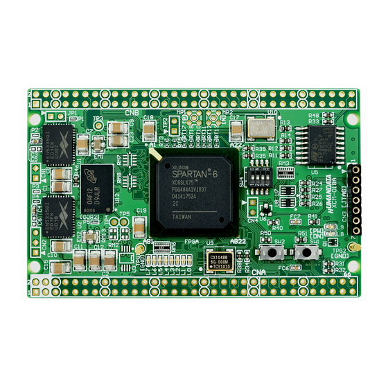
3. Overview 3.1. Name of Parts Oscillator 30 MHz User I/Os (CNB) Config. Device Config. Switch DDR2 SDRAM JTAG Serial I/F Status LEDs User LEDs User Switches User I/Os (CNA) Oscillator 50 MHz Component Side MRAM Solder Side XCM-018 Series v1.2... -
Page 8: Block Diagram
DDR 2 SDRAM (5 12Mbit) 5 0 MHz, 30MHz C l ock via MMCX MR A M (option) (4 Mbit) POR (240 ms typ.) Spartan-6 C onfig. Device U s er Switch XC6SLX 45/75/100/150 U s er LED -2FGG484C J TAG... -
Page 9: Clock
3.4. Clock 50 MHz (U9) and 30 MHz (U10) oscillators are equipped as on-board clock. External clock can be input from user I/O connectors (CNA, CNB) and MMCX connectors (MP1, MP2). For more details, please refer to circuit schematic. 3.5. JTAG Connector This connector is used to configure the FPGA and program the configuration device in-system. -
Page 10: Configuration Switch (Sw4)
3.6. Configuration Switch (SW4) The specification of configuration switch is below. “ON” means “Low (Ground)”. For each pins details, please refer to Spartan-6 configuration user guide. Net Label HSWAPEN ASW0 Default Function Pull-Up Configuration Mode User Master Serial/SPI JTAG M [0..1] value... -
Page 11: Fpga Configuration
4. FPGA Configuration To configure the FPGA via JTAG directly, select FPGA icon detected by Boundary-Scan and assign a bit-stream file. If configuration is completed successfully, the DONE LED will light up. 5. Configuration Device Programming To download a FPGA configuration data to the configuration device via JTAG, mcs file is required. -
Page 12: Additional Documentation And User Support
6. Additional Documentation and User Support The following documents and other supports are available at http://www.hdl.co.jp/en/spc/XCM/xcm-018/ Circuit Schematic Pin List Outline drawing Net List … and more. XCM-018 Series v1.2... - Page 13 Spartan -6 FPGA Board XCM-018 Series User’s Manual Ver. 1.2 ........... Nov. 14, 2016 HuMANDATA LTD. Address: 1-2-10-2F, Nakahozumi, Ibaraki Osaka, Japan ZIP 567-0034 Tel: 81-72-620-2002 (Japanese) Fax: 81-72-620-2003 (Japanese/English) URL: http://www.hdl.co.jp/en/ (Global) http://www.hdl.co.jp/ (Japan)
Need help?
Do you have a question about the Spartan-6 and is the answer not in the manual?
Questions and answers