Table of Contents
Advertisement
Quick Links
Advertisement
Table of Contents

Related Manuals for ADLINK Technology LEC-IMX6R2


Summary of Contents for ADLINK Technology LEC-IMX6R2
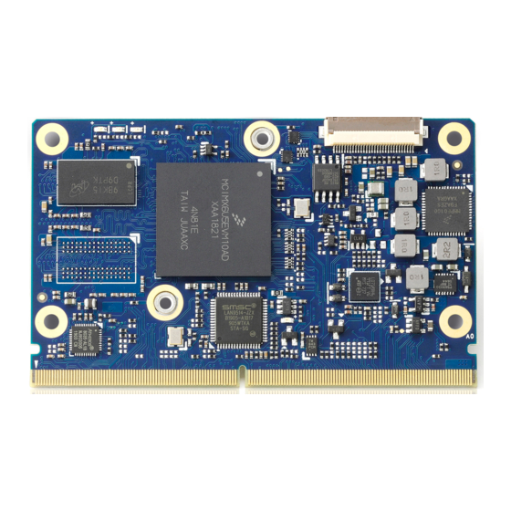
- Page 1 LEC-IMX6R2 02/12/2021...
- Page 2 Product names mentioned herein are used for identification purposes only and may be trademarks and/or registered trademarks of their respective companies. © Copyright 2017 ADLINK Technology, Incorporated This document contains proprietary information protected by copyright. All rights are reserved. No part of this manual may be reproduced by any mechanical, electronic, or other means in any form without prior written permission of the manufacturer.
- Page 3 Caution: This information indicates the possibility of minor physical injury, component damage, data loss, and/or program corruption. Warning: This information warns of possible serious physical injury, component damage, data loss, and/or program corruption. Page 3 copyright © 2021 ADLINK Technology Inc.
- Page 4 ADLINK Technology Inc. LEC-iMX6R2 User’s Guide Revision History Revision Description Date dd/mm/yyyy Author Initial public release 10/03/2021 Henri Parmentier Page 4 copyright © 2021 ADLINK Technology Inc.
-
Page 5: Table Of Contents
LAN ports ..................................................................37 4.3.9 SDIO ....................................................................39 4.3.10 SPI & ESPI ..................................................................40 4.3.11 SPI0 ....................................................................40 4.3.12 ESPI ....................................................................41 General Purpose I2C ................................................................42 4.4.1 GPIO....................................................................43 4.4.2 UART ....................................................................44 Page 5 copyright © 2021 ADLINK Technology Inc. - Page 6 SMARC pin to controller mapping ..........................................................50 5. Software Support ............................................................. 61 5.1.1 Uboot / Yocto ................................................................61 5.1.2 Ubuntu ................................................................... 61 5.1.3 Android ..................................................................61 6. Mechanical ..............................................................62 7. Thermal Solutions ............................................................ 63 Page 6 copyright © 2021 ADLINK Technology Inc.
- Page 7 LEC-iMX6R2 User’s Guide SGET SMARC Rev 2.1 List of Figures Figure 1 – Module function diagram ...................................................... 17 Figure 2 – Module top/botom side pin numbering ................................................. 18 Page 7 copyright © 2021 ADLINK Technology Inc.
-
Page 8: Introduction
Carrier Boards that implement other features such as audio CODECs, touch controllers, wireless devices, etc. The modular approach allows scalability, fast time to market and upgradability while still maintaining low costs, low power and small physical size. SMARC module and carrier specifications are available online at: https://www.sget.org/standards/smarc.html Page 8 copyright © 2021 ADLINK Technology Inc. -
Page 9: Specifications
• ECDH: FIPS SP800-56A Elliptic Curve Diffie-Hellman • NIST standard P256 elliptic curve support • SHA-256 & HMAC hash including off-chip context save/restore • AES-128: encrypt/decrypt, galois field multiply for GCM • Page 9 copyright © 2021 ADLINK Technology Inc. -
Page 10: Video
ADLINK Technology Inc. LEC-iMX6R2 User’s Guide 2.2 Video LEC-iMX6R2 standard display support is consisting of full HD capable HDMI 1.4, MIPI DSI and single/dual channel 24-bit LVDS. GPU Core: Vivante GC880 / GX2000 / GC2000+ • GPU cores are varying between SKU’s check datasheet for more info GPU/VPU Feature Support •... - Page 11 LEC-iMX6R2 User’s Guide SGET SMARC Rev 2.1 Camera support ▪ Single MIPI CSI camera supported on CSI1 ▪ Four lanes : QuadPlus, Quad, DualPlus, Dual ▪ Two lanes : DualLite and Solo Page 11 copyright © 2021 ADLINK Technology Inc.
-
Page 12: Audio
• Supports 10/100-Mbps data transfer rates, both full-duplex and half-duplex • Supports IEEE 802.1Q VLAN tag detection for reception frames • Support detection of LAN wake-up frames and AMD Magic Packet frames Page 12 copyright © 2021 ADLINK Technology Inc. -
Page 13: Extension Busses
2x CAN2.0B only or mixed CAN2.0B and CAN FB mode, data bit rate up to 8 Mbps via SPI to CAN controller 2 x SPI 2x I2S interfaces with audio resolution from 16-bits to 32-bits and sample rate up to 192KHz (see Audio Codec support) Page 13 copyright © 2021 ADLINK Technology Inc. -
Page 14: System Storage
1x SDIO (4-bit) compatible up to version 3.0. eMMC soldered on module 16, 32 or 64 GB (build option) either standard or -40+85C temp range Compatible with eMMC specification 4.41, 4.51 and 5.0 Page 14 copyright © 2021 ADLINK Technology Inc. -
Page 15: Sema® Board Management Controller
30-pin multipurpose flat cable connector for use with optional DB-30 debug module Provides JTAG, BMC access; UART, power test points; diagnostic LEDs, Power, Reset, Boot configuration 2.9 Boot Modes eMMC and SD-Card boot modes are supported Page 15 copyright © 2021 ADLINK Technology Inc. -
Page 16: Power
5-90% RH operating, non-condensing 5-95% RH storage (and operating with conformal coating) Shock and Vibration IEC 60068-2-64 and IEC-60068-2-27, MIL-STD-202 F, Method 213B, Table 213-I, Condition A and Method 214A, Table 214-I, Condition D Page 16 copyright © 2021 ADLINK Technology Inc. -
Page 17: Block Diagram
UART1 UART1 16/32/64GB UART2 UART2 UART3 UART3 I2S0 SDIO SDMMC GPIO GPIO x10 Crypto Auth. ATECC608A I2C_GP I2C_PM PMIC Watchdog / Boot Select, Power Control Lite Figure 1 – Module function diagram Page 17 copyright © 2021 ADLINK Technology Inc. -
Page 18: Pinout And Signal Descriptions
4. Pinout and Signal Descriptions 4.1 Pin Summary The below table is a comprehensible list of all signal pins on the MXM 3 connector in the standard specification SMARC 2.1. Those signals not supported on LEC-iMX6R2 are strikethrough STRIKETHROUGH P156 S156 Figure 2 –... - Page 19 USB3_SSRX+ GBE0_MDI0- PCIE_D_TX- / SERDES_1_TX- USB1+ USB3_SSRX- GBE0_MDI0+ GBE1_LINK_ACT# USB1- SPI0_CS1# PCIE_D_RX+ / SERDES_1_RX+ USB1_EN_OC# USB3+ note 2 PCIE_D_RX- / SERDES_1_RX- USB3- SDIO_WP USB2+ SDIO_CMD USB4+ USB2- USB2_SSTX+ SDIO_CD# USB4- USB2_EN_OC# USB2_SSTX- Page 19 copyright © 2021 ADLINK Technology Inc.
- Page 20 HDMI_CK+ / DP1_LANE3+ S102 DP0_LANE3+ P136 SER2_TX S137 LVDS0_3+ / eDP0_TX3+ / DSI0_D3+ P102 HDMI_CK- / DP1_LANE3- S103 DP0_LANE3- P137 SER2_RX S138 LVDS0_3- / eDP0_TX3- / DSI0_D3- P103 S104 USB3_OTG_ID P138 SER2_RTS# S139 I2C_LCD_CK Page 20 copyright © 2021 ADLINK Technology Inc.
- Page 21 S146 PCIE_WAKE# P155 VDD_IN S156 BATLOW# P146 CAN1_RX S147 VDD_RTC P156 VDD_IN S157 TEST# P147 VDD_IN S148 LID# S158 P148 VDD_IN S149 SLEEP# Note 1: Secondary LAN connected to the USB hub Page 21 copyright © 2021 ADLINK Technology Inc.
-
Page 22: Signal Terminology Descriptions
1.8V Power Domain: Active while CARRIER_PWRON is high and CARRIER_SBY# is NOT active (i.e. both signals are high) 3.3Vsb 3.3V Power Domain: Active while CARRIER_PWRON is high (regardless of CARRIER_SBY#) 1.8Vsb 1.8V Power Domain: Active while CARRIER_PWRON is high (regardless of CARRIER_SBY#) Page 22 copyright © 2021 ADLINK Technology Inc. -
Page 23: Signal Description By Function
LCD1_VDD_EN LCD1_VDD_EN S127 LCD0_BKLT_EN LCD0_BKLT_EN LCD0_BKLT_EN S107 LCD1_BKLT_EN LCD1_BKLT_EN LCD1_BKLT_EN S141 LCD0_BKLT_PWM LCD0_BKLT_PWM LCD0_BKLT_PWM S122 LCD1_BKLT_PWM LCD1_BKLT_PWM LCD1_BKLT_PWM S144 DSI0_TE eDP0_HPD S113 DSI1_TE eDP1_HPD S139 I2C_LCD_CK I2C_LCD_CK I2C_LCD_CK S140 I2C_LCD_DAT I2C_LCD_DAT I2C_LCD_DAT Page 23 copyright © 2021 ADLINK Technology Inc. - Page 24 Secondary panel power enable, active 1.8V Runtime high CMOS LCD1_BKLT_EN S107 Secondary panel backlight enable, active 1.8V Runtime high CMOS LCD1_BKLT_PWM S122 Secondary panel brightness control 1.8V Runtime through pulse width modulation (PWM) CMOS Page 24 copyright © 2021 ADLINK Technology Inc.
- Page 25 DDC data line used for flat panel detection and I/O OD 1.8V Runtime PU 2k2 control CMOS I2C_LCD_CK S139 DDC clock line used for flat panel detection and O OD 1.8V Runtime PU 2k2 control CMOS Page 25 copyright © 2021 ADLINK Technology Inc.
-
Page 26: Second & Third Display Interface
DP1_LANE3+ P101 DP0_LANE3+ P102 HDMI_CK- P102 DP1_LANE3- DP0_LANE3- S105 HDMI_CTRL_CK DP1_AUX+ S105 DP0_AUX+ S106 HDMI_CTRL_DAT DP1_AUX- S106 DP0_AUX- P104 HDMI_HPD DP1_HPD P104 DP0_HPD P107 DP1_AUX_SEL P107 DP0_AUX_SEL Note: DisplayPort is not supported Page 26 copyright © 2021 ADLINK Technology Inc. - Page 27 HDMI connector. HDMI_HPD P104 HDMI Hot plug active high detection 1.8V Standby Module must tolerate high level in stand-by mode signal that serves as an interrupt CMOS request Page 27 copyright © 2021 ADLINK Technology Inc.
-
Page 28: Mipi Camera Support
CAM0_RST# / P110 Camera 0 reset, active low output O CMOS 1.8V Runtime GPIO2 CAM_MCK Master clock output O CMOS 1.8V Runtime This signal is used by both CSI0 and CSI1 Page 28 copyright © 2021 ADLINK Technology Inc. - Page 29 Camera 0 reset, active low output O CMOS 1.8V Runtime CAM1_PWR# is default, GPIO3 can be enabled GPIO3 through DVT CAM_MCK Master clock output O CMOS 1.8V Runtime This signal is used by both CSI0 and CSI1 Page 29 copyright © 2021 ADLINK Technology Inc.
-
Page 30: I2S (Audio)
Module Input if CPU acts in Slave Mode AUDIO_MCK Master clock output to I2S 1.8V Runtime codec(s) CMOS Note: support for I2S1 signalling pins has been removed during update to SMARC 2.0 specification Page 30 copyright © 2021 ADLINK Technology Inc. -
Page 31: Usb Ports
LEC-iMX6R2 User’s Guide SGET SMARC Rev 2.1 4.3.5 USB ports Page 31 copyright © 2021 ADLINK Technology Inc. - Page 32 Carrier OD driver to indicate over-current situation. USB3+ USB differential data pairs for port 3 Runtime From USB HUB USB3- USB3_SSRX+ Receive signal differential pairs for USB SS Runtime USB3_SSRX- SuperSpeed on port 3 USB SS Page 32 copyright © 2021 ADLINK Technology Inc.
- Page 33 Pulled low by Module OD driver to disable USB0 power. Pulled CMOS 3.3V low by Carrier OD driver to indicate over-current situation. Note: USB0 is directly connected to the SOC, USB1/2/3/4 have shared bandwidth through a HUB, USB5 is not supported Page 33 copyright © 2021 ADLINK Technology Inc.
-
Page 34: Pcie Ports
I LVDS Runtime Series AC coupled off module PCIE_C_RX- PCIE PCIE_C_REFCK+ Differential PCIe Link C reference clock O LVDS Runtime PCIE_C_REFCK- output PCIE PCIE_C_RST# PCIe Port C reset output 3.3V Runtime CMOS Page 34 copyright © 2021 ADLINK Technology Inc. - Page 35 I OD 3.3V Runtime PU 10k common to PCIe links A, B, C, D CMOS Note: Module provides PCIe clock generators for PCIE_A so no external clock source on the carrier is needed Page 35 copyright © 2021 ADLINK Technology Inc.
-
Page 36: Sata Ports
Serial ATA channel 0, Receive Input differential pair. I SATA Runtime Series AC coupled on Module 10 nF SATA0_RX- SATA_ACT# SATA activity indicator O OD 3.3V Runtime Shall be able to sink 24mA or more Carrier LED CMOS current Page 36 copyright © 2021 ADLINK Technology Inc. -
Page 37: Lan Ports
Center-Tap reference voltage for Carrier board Ethernet Analog 0 to Runtime magnetic (if required by the Module GBE PHY) 3.3V max GBE0_SDP IEEE 1588 Trigger Signal. For hardware implementation 3.3V Runtime of PTP (precision time protocol) CMOS Page 37 copyright © 2021 ADLINK Technology Inc. - Page 38 Center-Tap reference voltage for Carrier board Ethernet Analog 0 to 3.3V Runtime magnetic `(if required by the Module GBE PHY)` GBE1_SDP IEEE 1588 Trigger Signal. For hardware implementation 3.3V Runtime of PTP (precision time protocol) CMOS Page 38 copyright © 2021 ADLINK Technology Inc.
-
Page 39: Sdio
SDIO_PWR_EN SDIO Power Enable. This signal is used to 3.3V Runtime should be driven low in STB Mode by the enable the power being supplied to a SD/MMC card CMOS module device. Page 39 copyright © 2021 ADLINK Technology Inc. -
Page 40: Spi & Espi
Note: SPI0 is free to use on the carrier but support only one device through CS0 SPI1 supports a CAN bus controller on the module through CS0, that leaves CS1 free for a device on the carrier Page 40 copyright © 2021 ADLINK Technology Inc. -
Page 41: Espi
In Single I/O mode, ESPI_IO_0 is the eSPI master output / eSPI slave input (MOSI) whereas ESPI_IO_1 is the SPI master input / eSPI slave output (MISO). Note: On NXP i.MX8M parts ECSPI is used (Enhanced Configurable Serial Peripheral Interface) Page 41 copyright © 2021 ADLINK Technology Inc. -
Page 42: General Purpose I2C
I2C clock for serial camera data support link MIPI CSI table I2C_PM_DAT P122 Power management I2C bus DATA (SMBus for x86) Power and System Management I2C_PM_CK P121 Power management I2C bus CLK (SMBus for x86) Power and System Management Page 42 copyright © 2021 ADLINK Technology Inc. -
Page 43: Gpio
PU 470K on the CMOS Module GPIO12 S142 General purpose I/O pin 1.8V Runtime PU 470K on the CMOS Module GPIO13 S123 General purpose I/O pin 1.8V Runtime PU 470K on the CMOS Module Page 43 copyright © 2021 ADLINK Technology Inc. -
Page 44: Uart
Four asynchronous serial ports are supported. The ports are designated SER0 – SER3. Ports SER0 and SER2 are 4 wire ports, (2 data - and 2 handshake lines). Ports SER1 and SER3 are 2 wire ports (data only). Page 44 copyright © 2021 ADLINK Technology Inc. -
Page 45: Can Bus
Module vendor specific test CMOS depended on particular module design. Carrier function(s). Board should leave this pin floating for normal operation WDT_TIME_OUT# S145 Watch-Dog-Timer Output, low 1.8V Runtime Driven only during runtime active. CMOS Page 45 copyright © 2021 ADLINK Technology Inc. -
Page 46: Power And System Management
Power-button input from Carrier board. Carrier I OD 1.8 to 5V Sleep PU 10k Driven by OD on Carrier. to float the line in in-active state. Active low, CMOS level sensitive. Should be debounced on the Module. Page 46 copyright © 2021 ADLINK Technology Inc. -
Page 47: Db30 Multipurpose Connector
4.4.6 DB30 Multipurpose Connector ➢ FPC Connector type : HIROSE,FH12-30S-0.5SH(55) DB30 connector brings out the following type of signals SPI0 bus JTAG to SOC Boot Select strap pins BMC programming interface Serial port Page 47 copyright © 2021 ADLINK Technology Inc. -
Page 48: Boot Select
SOC native Force Recovery mode – such as over a Serial Port. For x86 systems this signal may be used to load BIOS defaults. Pulled up on Module. Driven by OD part on Carrier. Page 48 copyright © 2021 ADLINK Technology Inc. -
Page 49: Power
S130, S136, S143, S158 VDD_RTC S147 Low current RTC circuit backup [2 to 3.25] / 3.25V power – 3.0V nominal. May be sourced from a Carrier based Lithium cell or Super Cap. Page 49 copyright © 2021 ADLINK Technology Inc. -
Page 50: Smarc Pin To Controller Mapping
GBE MDI AR8035-AL1B TRXN2 NVCC_RGMII GBE0_MDI2+ Bi-Dir GBE MDI AR8035-AL1B TRXP2 NVCC_RGMII GBE0_LINK_ACT# Out/OD CMOS/3.3V AR8035-AL1B LED_ACT NVCC_RGMII GBE0_MDI1- Bi-Dir GBE MDI AR8035-AL1B TRXN1 NVCC_RGMII GBE0_MDI1+ Bi-Dir GBE MDI AR8035-AL1B TRXP1 NVCC_RGMII GBE0_CTREF Page 50 copyright © 2021 ADLINK Technology Inc. - Page 51 Alt2 NVCC_EIM1 ESPI_IO_1 / SPI1_DIN CMOS/1.8V i.MX6 QP/Q/DP/D/DL/S EIM_OE Alt2 NVCC_EIM1 ESPI_IO_0 / SPI1_DO CMOS/1.8V i.MX6 QP/Q/DP/D/DL/S EIM_CS1 Alt2 NVCC_EIM1 USB0+ Bi-Dir i.MX6 QP/Q/DP/D/DL/S USB_OTG_DP VDD_USB_CAP USB0- Bi-Dir i.MX6 QP/Q/DP/D/DL/S USB_OTG_DN VDD_USB_CAP Page 51 copyright © 2021 ADLINK Technology Inc.
- Page 52 QP/Q/DP/D/DL/S PCIE_RXP PCIE_VPH PCIE_A_RX- serial-0R PCIe i.MX6 QP/Q/DP/D/DL/S PCIE_RXM PCIE_VPH PCIE_A_TX+ serial-0.1u PCIe i.MX6 QP/Q/DP/D/DL/S PCIE_TXP PCIE_VPH PCIE_A_TX- serial-0.1u PCIe i.MX6 QP/Q/DP/D/DL/S PCIE_TXM PCIE_VPH HDMI_D2+ / DP1_LANE0+ HDMI i.MX6 QP/Q/DP/D/DL/S HDMI_D2P HDMI_VPH Page 52 copyright © 2021 ADLINK Technology Inc.
- Page 53 P120 P121 I2C_PM_CK PU-1K I2C2 i.MX6 QP/Q/DP/D/DL/S EIM_EB2 Alt6 NVCC_EIM0 P122 I2C_PM_DAT Bi-Dir PU-1K I2C2 i.MX6 QP/Q/DP/D/DL/S EIM_D16 Alt6 NVCC_EIM0 P123 BOOT_SEL0# PU-4.7K CMOS/1.8V P124 BOOT_SEL1# PU-4.7K CMOS/1.8V P125 BOOT_SEL2# PU-4.7K CMOS/1.8V Page 53 copyright © 2021 ADLINK Technology Inc.
- Page 54 Alt2 NVCC_SD3 P147 VDD_IN P148 VDD_IN P149 VDD_IN P150 VDD_IN P151 VDD_IN P152 VDD_IN P153 VDD_IN P154 VDD_IN P155 VDD_IN P156 VDD_IN CSI1_TX+ / I2C_CAM1_CK PU-2.2K I2C1 i.MX6 QP/Q/DP/D/DL/S CSI0_DAT9 Alt4 NVCC_CSI Page 54 copyright © 2021 ADLINK Technology Inc.
- Page 55 Bi-Dir PU-49.9R RGMII LAN9514-JZX GBE1_MDI1- Bi-Dir PU-49.9R RGMII LAN9514-JZX GBE1_LINK1000# GBE1_MDI2+ GBE1_MDI2- GBE1_MDI3+ GBE1_MDI3- GBE1_CTREF PCIE_D_TX+ / SERDES_1_TX+ PCIE_D_TX- / SERDES_1_TX- GBE1_LINK_ACT# serial-0 RGMII LAN9514-JZX nLNKA_LED/GPIO1 PCIE_D_RX+ / SERDES_1_RX+ PCIE_D_RX- / SERDES_1_RX- Page 55 copyright © 2021 ADLINK Technology Inc.
- Page 56 Alt6 NVCC_EIM0 HDA_SYNC / I2S2_LRCK HDA_SDO / I2S2_SDOUT HDA_SDI / I2S2_SDIN HDA_CK / I2S2_CK SATA_ACT# CMOS/3.3V i.MX6 QP/Q/DP/D/DL/S DISP0_DAT23 Alt5 NVCC_LCD USB5_EN_OC# ESPI_IO_2 ESPI_IO_3 ESPI_RESET# CMOS/1.8V USB5+ USB5- USB3_SSTX+ USB3_SSTX- USB3_SSRX+ USB3_SSRX- Page 56 copyright © 2021 ADLINK Technology Inc.
- Page 57 USBDM4 USB2_SSTX+ USB2_SSTX- USB2_SSRX+ USB2_SSRX- PCIE_B_RST# PCIE_C_RST# PCIE_C_RX+ / SERDES_2_RX+ PCIE_C_RX- / SERDES_2_RX- PCIE_C_TX+ / SERDES_2_TX+ PCIE_C_TX- / SERDES_2_TX- PCIE_B_REFCK+ PCIE_B_REFCK- PCIE_B_RX+ PCIE_B_RX- PCIE_B_TX+ PCIE_B_TX- DP0_LANE0+ DP0_LANE0- DP0_AUX_SEL DP0_LANE1+ DP0_LANE1- DP0_HPD DP0_LANE2+ Page 57 copyright © 2021 ADLINK Technology Inc.
- Page 58 QP/Q/DP/D/DL/S LVDS1_TX2_N NVCC_LVDS_2P5 DSI1_D2- S119 S120 LVDS1_3+ / eDP1_TX3+ / LVDS i.MX6 QP/Q/DP/D/DL/S LVDS1_TX3_P NVCC_LVDS_2P5 DSI1_D3+ S121 LVDS1_3- / eDP1_TX3- / LVDS i.MX6 QP/Q/DP/D/DL/S LVDS1_TX3_N NVCC_LVDS_2P5 DSI1_D3- S122 LCD1_BKLT_PWM S123 GPIO13 S124 Page 58 copyright © 2021 ADLINK Technology Inc.
- Page 59 S146 PCIE_WAKE# CMOS/1.8V i.MX6 QP/Q/DP/D/DL/S CSI0_DATA_EN Alt5 NVCC_CSI S147 VDD_RTC S148 LID# PU-4.7K CMOS/1.8V i.MX6 QP/Q/DP/D/DL/S GPIO_7 Alt5 NVCC_GPIO S149 SLEEP# PU-4.7K CMOS/1.8V i.MX6 QP/Q/DP/D/DL/S NANDF_D7 Alt5 NVCC_NANDF S150 VIN_PWR_BAD# PU-10K CMOS/1.8V Page 59 copyright © 2021 ADLINK Technology Inc.
- Page 60 S154 CARRIER_PWR_ON_B (BMC) CMOS/1.8V S155 FORCE_RECOV_B PU-4.7K CMOS/1.8V i.MX6 QP/Q/DP/D/DL/S BOOT_MODE0/1 Alt0 VDD_SNVS_IN S156 BATLOW_B PU-68K CMOS/1.8V i.MX6 QP/Q/DP/D/DL/S NANDF_RB0 Alt5 NVCC_NANDF S157 TEST_B PU-4.7K CMOS/1.8V i.MX6 QP/Q/DP/D/DL/S GPIO_8 Alt5 NVCC_GPIO S158 Page 60 copyright © 2021 ADLINK Technology Inc.
-
Page 61: Software Support
Goto : https://github.com/adlink Yocto source-code and compiling instructions are available 5.1.2 Ubuntu Build instruction from source, are available on Github 5.1.3 Android Goto : https://github.com/adlink Android source-code and compiling instructions are available Page 61 copyright © 2021 ADLINK Technology Inc. -
Page 62: Mechanical
ADLINK Technology Inc. LEC-iMX6R2 User’s Guide 6. Mechanical Page 62 copyright © 2021 ADLINK Technology Inc. -
Page 63: Thermal Solutions
LEC-iMX6R2 User’s Guide SGET SMARC Rev 2.1 7. Thermal Solutions 7.1.1 Heatsink : THS 2.7mm x 4pcs Page 63 copyright © 2021 ADLINK Technology Inc. - Page 64 7.1.2 Heatspreader : HTS M3 x 4pcs 2.7mm x 4pcs HTS-sIMX6R2-SDL Heatspreader for LEC-iMXR2 solo/Duallite THS-sIMX6R2-SDL Low profile heatsink for LEC-iMX6R2 Solo/DualLite HTS-sIMX6R2-DQP Heatspreader for LEC-iMX8R2 Dual/Quad THS-sIMX6R2-DQP Low profile heatsink for LEC-iMX6R2 with Dual/Quad Page 64 copyright © 2021 ADLINK Technology Inc.
- Page 65 LEC-iMX6R2 User’s Guide SGET SMARC Rev 2.1 Page 65 copyright © 2021 ADLINK Technology Inc.
Need help?
Do you have a question about the LEC-IMX6R2 and is the answer not in the manual?
Questions and answers