
Related Manuals for ADLINK Technology LEC-BASE 2.0


Summary of Contents for ADLINK Technology LEC-BASE 2.0
- Page 1 LEC-BASE 2.0 Technical Reference Low Energy Computer-On-Module Carrier Manual Rev.: Revision Date: April 19, 2018 Part Number: 50-1Z232-1000 Leading EDGE COMPUTING...
- Page 2 Audience This manual provides reference only for computer design engineers, including but not limited to hardware and software designers and applications engineers. ADLINK Technology, Inc. assumes you are qualified to design and implement prototype computer equipment. Preface...
- Page 3 LEC-BASE 2.0 Environmental Responsibility ADLINK is committed to fulfill its social responsibility to global environmental preservation through compliance with the European Union's Restriction of Hazardous Substances (RoHS) directive and Waste Electrical and Electronic Equipment (WEEE) directive. Environmental protection is a top priority for ADLINK. We have enforced measures to ensure that our prod- ucts, manufacturing processes, components, and raw materials have as little impact on the environment as possible.
- Page 4 Conventions The following conventions may be used throughout this manual, denoting special levels of information. This information adds clarity or specifics to text and illustrations. This information indicates the possibility of minor physical injury, component damage, data loss, and/or program corruption. This information warns of possible serious physi- cal injury, component damage, data loss, and/or program corruption.
-
Page 5: Table Of Contents
LEC-BASE 2.0 Table of Contents Preface ..........................ii 1 Product Overview ......................1 Carrier Description .........................1 Features ..........................2 Ordering Information ......................3 Block Diagram ........................4 Specifications ......................... 5 1.5.1 Physical ........................5 1.5.2 Electrical ........................5 1.5.3 Environmental ........................ 5 1.5.4... - Page 6 Display Interfaces ........................ 30 3.3.1 LVDS (CN25) ......................30 3.3.2 LVDS Backlight 0 (CN116) ..................31 3.3.3 LVDS Backlight 1 (CN113) ..................32 3.3.4 LVDS VCC Voltage Select (CN114) ................32 3.3.5 LVDS VDD Voltage Select (CN117) ................33 3.3.6 LVDS / eDP Mode Select (CN120) ................
- Page 7 LEC-BASE 2.0 3.10 SPI Interfaces ........................48 3.10.1 SPI0 Voltage Select (CN145) ..................48 3.10.2 SPI0 Flash Socket (CN146) ..................48 3.10.3 eSPI / SPI1 Voltage Select (CN147) ................49 3.10.4 SPI0 Interface (CN148) ....................49 3.10.5 SPI0 CS0/CS1 Select (CN149) ................... 49 3.10.6 eSPI / SPI1 Interface (CN150) ..................50...
- Page 8 This page intentionally left blank. viii Table of Contents...
-
Page 9: Product Overview
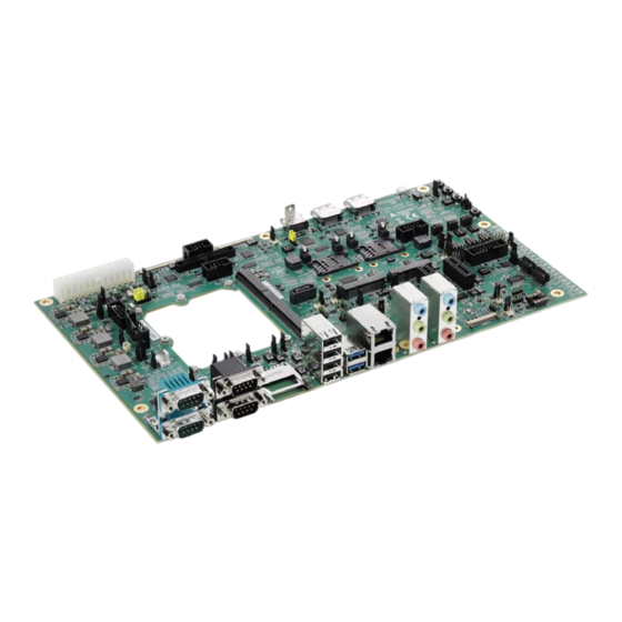
Carrier Specifications Carrier Description The ADLINK LEC-BASE 2.0 is a host carrier board for ADLINK’s SMARC modules and serves as reference design for SMARC modules conforming to the SMARC 2.0 specification. The SMARC module plugs directly into the LEC-BASE 2.0 where the carrier board becomes a design platform for testing and developing your applications. -
Page 10: Features
Features SMARC interface MXM3 connector PCI Express Bus 2x PCIe x1 slots 2x PCIe Mini slots Serial Port UART interfaces (4x UART) Null Modem RS-232 on serial ports COM0 - COM3 2-wire and 4-wire connectors ... -
Page 11: Ordering Information
Sleep Button Test Button LID Switch Boot Select Switch Ordering Information Table 1-1: LEC-BASE 2.0 Models Model Number Description SMARC evaluation carrier board for SMARC 2.0 compliant mod- LEC-BASE 2.0 ules (91-77A05-000E or higher) Product Overview... -
Page 12: Block Diagram
Block Diagram Figure 1-2 presents a functional representation of the carrier. 3.0V to 5.25V Power SD/SDIO 4-bit GbE0 GbE1 Batman SATA (Gen1,2,3) USB0 (2.0) SPI0 and SPI/eSPI1 USB2 (2.0/3.0) USB1 (2.0) Misc USB3 (2.0/3.0) HDMI/DP++ USB4 (2.0) SC/DC LVDS (18/24bit)/eDP0/1 USB5 (2.0) SM AR C 2.0 M odule... -
Page 13: Specifications
Most components on the LEC-BASE 2.0 carrier are selected as extended temperature range parts (-40°C to +85°C). Some components are not available in this temperature range. In these cases, the component temperature ranges are narrower. The LEC-BASE 2.0 is validated in the -40°C to +85°C range. -
Page 14: Mechanical
Figure 1-3 provides the mechanical dimensions and mounting hole sizes of the LEC-BASE 2.0. The LEC-BASE 2.0 can be mounted to a chassis using M4, B-head screws. Mezzanine cards can be mounted to the carrier using female-female standoffs with M2.5 threads and M2.5, B-head screws. -
Page 15: Hardware
Hardware This chapter describes the physical specifications of the interface connectors, headers, LEDs, and switches on the LEC-BASE 2.0. The second section of this chapter, titled Standard Hard- ware References, further describes the industry standard IO hardware on the carrier. - Page 16 Table 2-1: Header, Switch, LED, and Connector Descriptions (Continued) Signal / Device Pinout Link Description Designator CN120 LVDS / eDP Mode Select Table 3-24 6-pin, 2.0mm jumper header for selecting between LVDS and embedded DisplayPort display modes [NELTRON, 2208SM-06G-CR] CN121 eDP0 Table 3-26 40-pin, 0.50mm right-angle, standard connector for...
- Page 17 LEC-BASE 2.0 Table 2-1: Header, Switch, LED, and Connector Descriptions (Continued) Signal / Device Pinout Link Description Designator CN138 USB11 Wake / No Wake Table 3-1 3-pin, 2.0mm jumper header to select between Wake Select and No Wake from sleep states for the USB11 port [JIH21N12050-03S10B-01G-4/2.8-G]...
- Page 18 Table 2-1: Header, Switch, LED, and Connector Descriptions (Continued) Signal / Device Pinout Link Description Designator CN156 Mic BIAS Select Table 3-66 3-pin, 2.0mm jumper header to select between Internal and External Mic BIAS for the I2S Audio interface [JIH21N12050-03S10B-01G-4/2.8-G] CN157 I2S Audio Codec Select Table 3-67...
- Page 19 LEC-BASE 2.0 Table 2-1: Header, Switch, LED, and Connector Descriptions (Continued) Signal / Device Pinout Link Description Designator CN183 PCIe A Table 3-85 36-pin, 1.0mm standard connector for PCI Express x1, Port A [FOXCONN, 2EG01827-D2D-DF] CN184 mPCIe B “PCIe Mini 52-pin, 0.8mm standard, right-angle slot for PCI...
- Page 20 Table 2-1: Header, Switch, LED, and Connector Descriptions (Continued) Signal / Device Pinout Link Description Designator CN201 PCIe ClockBuffers 0-1 Table 3-91 6-pin, 2.0mm jumper header for connecting one of Connect the two PCIe ClockBuffers (0 or 1) to the SMBus [NELTRON, 2208SM-06G-CR] CN202 BattMan Charger...
- Page 21 LEC-BASE 2.0 Table 2-1: Header, Switch, LED, and Connector Descriptions (Continued) Signal / Device Pinout Link Description Designator LED20 USB3, VBUS On Green LED indicating Vbus is applied to USB3 Applicable [LIGITEK, LG-192G-CT] LED21 USB0, VBUS On Green LED indicating Vbus is applied to USB0...
- Page 22 Table 2-1: Header, Switch, LED, and Connector Descriptions (Continued) Signal / Device Pinout Link Description Designator SW36 Sleep, module Push-button switch to induce module sleep mode Applicable [CONTACT, TS-A02-2, BLACK] SW37 Toggle switch to assert LID function on module Applicable [NKK, G12AP, BLACK] SW38 Test...
- Page 23 LEC-BASE 2.0 SW35 SW34 SW36 SW37 SW38 CN210 CN209 SW68 SW72 CN147 CN159 SW73 SW69 SW71 SW74 SW52 CN149 CN196 CN145 CN195 CN127 CN186 CN185 CN183 CN154 CN182 CN125 CN157 CN106 CN120 CN130 CN107 CN158 CN211 CN141 CN143 CN212 CN162...
- Page 24 CONNECTORS LEDs CN158 - SMARC Interface BT2 - Battery Socket CN159 - USB0 Wake/NoWake Select CN2 - ATX Power Input LED15 - USB12, VBUS_ON CN160 - USB0 2.0 OTG Interface CN25 - LVDS, Dual-Channel Interface LED16 - USB4, VBUS_ON CN162 - USB3 Wake/NoWake Select CN105 - I2C_GP Interface LED17 - USB11, VBUS_ON CN163 - GPIO 0-3 Enable...
- Page 25 LEC-BASE 2.0 Figure 2-3 illustrates the faces of the standard interface connectors mounted along one edge of the carrier. These connectors are for CAN, Serial Port, SD Card, USB, Ethernet, Audio, and MIPI-CSI Camera (conforming to the QSeven 2.1 Specification) cable connectors.
-
Page 26: Standard Hardware References
2.2.1 Audio IO Jacks The LEC-BASE 2.0 provides two standard audio jacks for HD (CN153) and I2S (CN155) audio. Two audio codecs support these two interfaces. Figure 2-5 depicts the three lines of the audio jacks: Line In (1 - Blue), Line Out (2 - Green), and MIC In (3 - Pink). Figure 2-6 presents the functional block diagram of I2S and HDA signals connections from the SMARC module to the audio components on the carrier. -
Page 27: Pcie Mini Card Slot
2.2.2 PCIe Mini Card Slot The LEC-BASE 2.0 provides two standard PCI Express Mini Card slots. Figure 2-7 presents one mini card slot with one of the two fastening latches. Figure 2-8 illustrates the functional block diagram of the PCIe Mini Card signals and hardware on the carrier. -
Page 28: Sd Card Slot
2.2.3 SD Card Slot The SD Card slot (CN151) provides the standard 4-bit, push-push interface for SD memory cards. LED5 provides indication of SD power. UHS cards with 1.8V data signaling are sup- ported. The card supply is always 3.3V regardless if either 1.8V signaling or 3.3V signaling is com- mitted by both card controllers. -
Page 29: Sim Slots
LEC-BASE 2.0 2.2.4 SIM Slots Two SIM slots (CN182 / CN185) provide interface for two Subscriber Identity Modules, support- ing both PCIe Mini Card slots: CN182 (SIM1) supports the CN184 Mini Card slot and CN185 (SIM2) supports the CN192 Mini Card slot. Figure 2-10 illustrates the slots’ hinge-type connec- tions. -
Page 30: Battery Socket
Table 2-4: SIM2 Slot (CN185) Pin # Signal Description Scheme UM2_PWR +1.8V or +3V VDC power supply input (depending on PCIe Mini Card; +5V is supported if supplied by CN185 the Mini Card) UIM2_CLK UIM2_DAT UIM2_RST UIM2_VPP UM2_RESET Resets the card’s UIM2_PWR communications SIM-CARD_6... -
Page 31: Interfaces
USB Interfaces All USB interfaces on the LEC-BASE 2.0 are supported through standard connectors, and their signal definitions can be found in their respective specifications. Sections 3.1.1 through 3.1.11 provide the pinout tables for all the supporting USB jumper headers on the carrier. Refer to the following block diagram for an illustration of the USB interface map on the carrier. -
Page 32: Usb11 Wake / No Wake Select (Cn138)
3.1.1 USB11 Wake / No Wake Select (CN138) Table 3-53 lists the pin signals of the USB11 Wake / No Wake select jumper header, which pro- vides 3 pins in a single row with 2.00mm pitch. Table 3-1: USB11 Wake / No Wake Select (CN138) Pin # Signal Jumper Positions... -
Page 33: Usb5 Wake / No Wake Select (Cn143)
LEC-BASE 2.0 3.1.5 USB5 Wake / No Wake Select (CN143) Table 3-5 lists the pin signals of the USB5 Wake / No Wake select jumper header, which pro- vides 3 pins in a single row with 2.00mm pitch. Table 3-5: USB5 Wake / No Wake Select (CN143) -
Page 34: Usb5 2.0 Over-Current Detection Source Select (Cn212)
3.1.9 USB5 2.0 Over-Current Detection Source Select (CN212) Table 3-53 lists the pin signals of the USB5 2.0 Over-Current Detection Source Select jumper header, which provides 3 pins in a single row with 2.00mm pitch. Table 3-9: USB5 2.0 Over-Current Detection Source Select (CN212) Pin # Signal Jumper Positions... -
Page 35: Power Interfaces
LEC-BASE 2.0 Power Interfaces This section describes the signals for all power interfaces on the carrier, including ATX, RTC battery, and Smart Battery (BattMan) input interfaces. 3.2.1 ATX Power (CN2) Table 3-12 lists the signals of the standard ATX Power connector, which provides 24 pins, 2 rows consecutive pin sequence (1, 13) with 4.20mm pitch. -
Page 36: Battery Interface (Cn111)
3.2.2 Battery Interface (CN111) Table 3-13 lists the pin signals of the battery interface header, which provides 2 pins in a single row with 1.25mm pitch. Table 3-13: Battery Interface (CN111) Pin # Signal +VDD_RTC_IN NOTE: Shaded table cells denote power or ground. 3.2.3 Battery Enable (CN110) Table 3-14 lists the pin signals of the RTC battery enable jumper header, which provides 2 pins... -
Page 37: Battman Smbus Voltage Select (Cn129)
LEC-BASE 2.0 3.2.5 BattMan SMBus Voltage Select (CN129) Table 3-16 lists the pin signals of the BattMan SMBus voltage select jumper header, which pro- vides 3 pins in a single row with 2.00mm pitch. Table 3-16: BattMan SMBus Voltage Select (CN129) -
Page 38: Display Interfaces
Display Interfaces The LEC-BASE 2.0 supports four display interfaces, with the capacity to use three of them, simultaneously. This section provides the pinout tables for all four interfaces including the pinout tables for all support interfaces and jumper headers. The following list presents the four display interfaces. -
Page 39: Lvds Backlight 0 (Cn116)
LEC-BASE 2.0 Table 3-19: LVDS Interface Pin Signals (CN25) (Continued) Pin # Signal Description SMARC Signal Ground LVDS_B1_N Data Negative Output - Channel B LVDS1_1- LVDS_B1_P Data Positive Output - Channel B LVDS1_1+ Ground LVDS_B2_N Data Negative Output - Channel B... -
Page 40: Lvds Backlight 1 (Cn113)
3.3.3 LVDS Backlight 1 (CN113) Table 3-21 lists the pin signals of the LVDS Backlight 1 interface, which provides 8 pins, 2 rows, odd/even pin sequence (1, 2) and 2.54mm pitch. with Table 3-21: LVDS Backlight 1 (CN113) Pin # Signal +VDD_PANEL (VDD fixed voltages 3.3V or 5V selected at CN117;... -
Page 41: Lvds Vdd Voltage Select (Cn117)
LEC-BASE 2.0 3.3.5 LVDS VDD Voltage Select (CN117) Table 3-22 lists the pin signals of the LVDS VDD Voltage Select jumper header, which provides 6 pins in two rows with odd/even pin sequence (1,2) and 2mm pitch. Table 3-23: LVDS Voltage Select Signals (CN117) - Page 42 Table 3-26: eDP0 Video Signals (CN121) (Continued) Pin # Signal Description eDP0_BKLT_ENABLE Backlight power enable eDP0_BKLT_GND Backlight ground eDP0_BKLT_GND Backlight ground eDP0_BKLT_GND Backlight ground eDP0_BKLT_GND Backlight ground eDP0_HPD Hot Plug Detect eDP0_LCD_GND LCD ground eDP0_LCD_GND LCD ground eDP0_LCD_GND LCD ground eDP0_LCD_GND LCD ground Not Connected...
-
Page 43: Edp1 (Cn118)
LEC-BASE 2.0 3.3.9 eDP1 (CN118) Table 3-27 lists the pin signals of the embedded DisplayPort 1 connector, which provides 40- pins, single row with 0.5mm pitch. Table 3-27: eDP1 Video Signals (CN118) Pin # Signal Description Not Connected eDP1_BKLT_PWR Backlight power (5V / 12V [selected at CN207]) -
Page 44: Hdmi (Cn123)
3.3.10 HDMI (CN123) Table 3-31 lists the pin signals of the HDMI interface, which provides a 19-pin, standard two-row connector with 0.5mm pitch. Table 3-28: HDMI Signals (CN123) Pin # Signal Description Pin Sequence HDMI_D2_P Data2 differential signal - Positive Data2 Ground HDMI_D2_N Data2 differential signal - Negative... -
Page 45: Hdmi / Dp1 Mode Select (Cn125)
LEC-BASE 2.0 3.3.12 HDMI / DP1 Mode Select (CN125) Table 3-30 lists the pin signals of the HDMI/DP1 Mode Select jumper header, which provides 5 pins in a single row with 2.00mm pitch. Table 3-30: HDMI / DP1 Mode Select (CN125) -
Page 46: Displayport++ 1 (Cn124)
NOTE: The shaded table cells denote power or ground. I2C Interfaces The LEC-BASE 2.0 supports I2C interfaces for General Purpose, Camera, and Power Manage- ment. This section provides the pinout tables for all I2C interfaces including the pinout tables for all support interfaces and jumper headers. -
Page 47: I2C Cam0 (Cn106)
LEC-BASE 2.0 3.4.2 I2C CAM0 (CN106) Table 3-33 lists the pin signals of the I2C CAM0 header, which provides 4 pins in a single row with 2.00mm pitch. Table 3-34: I2C CAM0 (CN106) Pin # Signal I2C_CAM0_CK Ground +VCC_CAM0_GP I2C_CAM0_DAT NOTE: Shaded table cells denote ground or power. -
Page 48: I2C Eeprom Socket (Cn194)
3.4.5 I2C EEPROM Socket (CN194) Table 3-37 lists the pin signals of the I2C EEPROM socket, which provides 8 pins in two rows with consecutive pin sequence (1,8) and 2.54mm pitch. Table 3-37: I2C EEPROM Socket (CN194) Pin # Signal Pin # Signal CR_I2C_A0... -
Page 49: I2C_Cam0 Voltage Select (Cn197)
LEC-BASE 2.0 3.4.8 I2C_CAM0 Voltage Select (CN197) Table 3-40 lists the pin signals of the I2C_CAM0 Voltage Select jumper header, which provides 6 pins in two rows with odd/even pin sequence (1,2) and 2.00mm pitch. Table 3-40: I2C_CAM0 Voltage Select (CN197) -
Page 50: Fan Voltage Select (Cn112)
3.5.2 Fan Voltage Select (CN112) Table 3-43 lists the pin signals of the Fan Voltage Select jumper header, which provides 3 pins in a single row with 2mm pitch. Table 3-43: Fan Voltage Select (CN112) Pin # Signal Jumper Positions +V12P0_ATX •... -
Page 51: Gpio Camera Interface (Cn127)
Table 3-45: GPIO Camera Interface (CN127) Pin # Signal CAM0_GPIO CAM1_GPIO These two GPIOs follow the SGET Q7 specifica- tion 2.1. They can be used by camera add-on cards for user-specified camera functions. Not supported by the ADLINK LEC-BASE 2.0 camera add-on card. Interfaces... -
Page 52: Ieee 1588 Trigger Interface (Cn130)
IEEE 1588 Trigger Interface (CN130) Table 3-46 lists the pin signals of the IEEE 1588 Precision Time Protocol trigger interface, which provides 4 pins in two rows with odd/even pin sequence (1,2) and 2.54mm pitch. Table 3-46: IEEE 1588 Trigger Interface (CN130) Pin # Signal Pin #... -
Page 53: Com1 (Cn134 [Bottom])
LEC-BASE 2.0 3.8.2 COM1 (CN134 [bottom]) Table 3-48 lists the signals of the COM1, 2-wire RS232 interface, which provides a standard DB9 connector. Table 3-48: COM1 Signals (CN134 [bottom]) Pin # Signal Pin Sequence Not Connected COM1_RX COM1_TX Not Connected... -
Page 54: Serial Voltage Mode Select (Cn204)
3.8.5 Serial Voltage Mode Select (CN204) Table 3-51 lists the pin signals of the Serial Voltage Mode select jumper header, which provides 3 pins in a single row with 2.00mm pitch. Table 3-51: Serial Voltage Mode Select (CN204) Pin # Signal Jumper Positions +V1P8S... -
Page 55: Can1 (Cn136 [Bottom])
LEC-BASE 2.0 3.9.3 CAN1 (CN136 [bottom]) Table 3-54 lists the signals of the Controller Area Network interface, CAN1, which provides a standard DB9 connector. Table 3-54: CAN1 Signals (CN136 [bottom]) Pin # Signal Pin Sequence Not Connected CAN1_L GND_CAN Not Connected... -
Page 56: 3.10 Spi Interfaces
3.10 SPI Interfaces 3.10.1 SPI0 Voltage Select (CN145) Table 3-56 lists the pin signals of the SPI0 Voltage Select jumper header, which provides 3 pins in a single row with 2.54mm pitch. Table 3-56: SPI0 Voltage Select (CN145) Pin # Signal Jumper Positions +V1P8S... -
Page 57: Espi / Spi1 Voltage Select (Cn147)
LEC-BASE 2.0 3.10.3 eSPI / SPI1 Voltage Select (CN147) Table 3-58 lists the pin signals of the eSPI / SPI1 Voltage Select jumper header, which provides 3 pins in a single row with 2.54mm pitch. Table 3-58: eSPI / SPI1 Voltage Select (CN147) -
Page 58: Espi / Spi1 Interface (Cn150)
3.10.6 eSPI / SPI1 Interface (CN150) Table 3-59 lists the pin signals of the eSPI / SPI1 interface, which provides 16 pins in two rows with odd/even pin sequence (1,2) and 2.54mm pitch. Table 3-61: eSPI / SPI1 Interface (CN150) Pin # Signal Pin #... -
Page 59: Sd Card Power Mode Select (Cn152)
[default] 3.12 Audio Interfaces Two audio interfaces (HD and I2S) on the LEC-BASE 2.0 are supported through standard con- nectors, and their signal definitions can be found in the Standard Hardware References section of Chapter 2. This section provides the pinout tables for all the supporting audio jumper head- ers. -
Page 60: 3.13 Gpio Interfaces
3.13 GPIO Interfaces Twelve GPIO ports support general purpose IO signals on three header interfaces. This section defines the signals of all three headers as well as the signals of all GPIO support jumper head- ers. 3.13.1 GPIO 0-3 Interface (CN167) Table 3-68 lists the pin signals of the GPIO 0-3 interface, which provides 10 pins in two rows with odd/even pin sequence (1,2) and 2.54mm pitch. -
Page 61: Gpio 4-7 Interface (Cn173)
LEC-BASE 2.0 3.13.4 GPIO 4-7 Interface (CN173) Table 3-71 lists the pin signals of the GPIO 4-7 interface, which provides 10 pins in two rows with odd/even pin sequence (1,2) and 2.54mm pitch. Table 3-71: GPIO 4-7 Interface (CN173) Pin #... -
Page 62: Gpio 8-11 Interface (Cn179)
3.13.7 GPIO 8-11 Interface (CN179) Table 3-74 lists the pin signals of the GPIO 8-11 interface, which provides 10 pins in two rows with odd/even pin sequence (1,2) and 2.54mm pitch. Table 3-74: GPIO 8-11 Interface (CN179) Pin # Signal Pin # Signal +V1P8S... -
Page 63: Gpio5 Fan Power Management Enable (Cn199)
LEC-BASE 2.0 3.13.10 GPIO5 Fan Power Management Enable (CN199) Table 3-77 lists the pin signals of the GPIO5 Fan PWM Out enable jumper header, which pro- vides 3 pins in a single row with 2.00mm pitch. Table 3-77: GPIO5 Fan PWM Out Enable (CN199) -
Page 64: Gpio 4-7, 2.2K Pu Configuration Switch (Sw69)
3.13.13 GPIO 4-7, 2.2K PU Configuration Switch (SW69) Table 3-80 lists the pin signals of the GPIO 4-7, 2.2K PU configuration dip switch, which pro- vides 4 poles, 8 pin positions with 1.27mm pitch. Table 3-80: GPIO 4-7, 2.2K PU Configuration Switch (SW69) Position Signal Position... -
Page 65: Gpio 4-7, 10K Pu Configuration Switch (Sw73)
LEC-BASE 2.0 3.13.16 GPIO 4-7, 10K PU Configuration Switch (SW73) Table 3-83 lists the pin signals of the GPIO 4-7, 10K PU configuration dip switch, which provides 4 poles, 8 pin positions with 1.27mm pitch. Table 3-83: GPIO 4-7, 10K PU Configuration Switch (SW73) -
Page 66: Pcie D X1 (Cn186)
Table 3-85: PCIe A x1 (Continued) (CN183) (Continued) Signal Signal B10 +3VP3_SBY +3VP3S B11 PCIE_WAKE_A# PCIE_A_RST# B12 Not Connected B13 GND REFCLK_A_P B14 PCIE_A_TXC_P REFCLK_A_N B15 PCIE_A_TXC_N B16 GND PCIE_A_RX_P B17 PCIE_PRSNT_A# PCIE_A_RX_N B18 GND NOTE: Shaded table cells denote power or ground. The # symbol indicates the signal is Active Low. -
Page 67: Expansion Interface - Mpcie B (Cn193)
LEC-BASE 2.0 3.14.3 Expansion Interface - mPCIe B (CN193) Table 3-87 lists the pin signals of the mini PCIe B expansion interface, which provides 8 pins in two rows with odd/even pin sequence (1,2) and 2.00mm pitch. Table 3-87: Expansion Interface - mPCIe B (CN193) -
Page 68: Pcie Re-Driver Socket (U174)
3.14.6 PCIe Re-Driver Socket (U174) Table 3-90 lists the pin signals of the PCIe Re-driver socket, which provides 8 pins in two rows with consecutive pin sequence (1,8) and 1.27mm pitch. Table 3-90: PCIe Re-driver Socket (U174) Pin # Signal Pin # Signal PCIE_RD_ROM_A0... -
Page 69: 3.15 Miscellaneous Interfaces
LEC-BASE 2.0 3.15 Miscellaneous Interfaces 3.15.1 SMBus ClockBuffers 0-1 Connect (CN201) Table 3-91 lists the pin signals of the SMBus ClockBuffers 0-1 connect jumper header, which provides 6 pins in two rows with odd/even pin sequence (1,2) and 2.00mm pitch. -
Page 70: Pll Bandwidth Configuration Switch (Sw66)
3.15.3 PLL Bandwidth Configuration Switch (SW66) Table 3-94 lists the pin signals of the PLL Bandwidth configuration dip switch for PCIe Clock- Buffer components, providing 2 poles and 4 pin positions. Table 3-94: PLL Bandwidth Configuration Switch (SW66) Position Position Signal Signal 1 (off) -
Page 71: Appendix A Technical Support
LEC-BASE 2.0 Appendix A Technical Support ADLINK Technology, Inc. provides a number of methods for contacting Technical Support listed in Table A-1 below. Requests for support through Ask an Expert are given the highest priorities, and usually will be addressed within one working day. - Page 72 Table A-1: Technical Support Contact Information (Continued) Method Contact Information Address: Hans-Thoma-Strasse 11 D-68163 Mannheim, Germany Tel: +49-621-43214-0 Fax: +49-621 43214-30 Email: emea@adlinktech.com Please visit the contact page using the web site link shown above for information on how to contact the ADLINK regional office near- est you.
Need help?
Do you have a question about the LEC-BASE 2.0 and is the answer not in the manual?
Questions and answers