
Related Manuals for ADLINK Technology LEC-BT


Summary of Contents for ADLINK Technology LEC-BT
- Page 1 LEC-BT (Low Energy Computer on Module) Technical Reference P/N 50-1Z166-1020 Rev 3.00 Advance Technologies. Automate the World.
- Page 2 © Copyright 2014, 2015, 2016 ADLINK Technology, Incorporated Audience This manual provides reference only for computer design engineers, including but not limited to hardware and software designers and applications engineers. ADLINK Technology, Inc. assumes you are qualified to design and implement prototype computer equipment. Preface...
- Page 3 LEC-BT Environmental Responsibility ADLINK is committed to fulfill its social responsibility to global environmental preservation through compliance with the European Union's Restriction of Hazardous Substances (RoHS) directive and Waste Electrical and Electronic Equipment (WEEE) directive. Environmental protection is a top priority for ADLINK. We have enforced measures to ensure that our prod- ucts, manufacturing processes, components, and raw materials have as little impact on the environment as possible.
- Page 4 Preface...
-
Page 5: Table Of Contents
LEC-BT Table of Contents 1 Overview ........................... 1 Block Diagram........................1 Major Components (ICs)......................2 Connectors, Switches, and LEDs ..................4 Specifications......................... 6 1.4.1 Physical Specifications ......................6 1.4.2 Mechanical Specifications ....................6 1.4.3 Electrical Specifications .....................7 1.4.4 Power Specifications ......................7 1.4.5 Environmental Specifications.....................7 1.4.6 Thermal/Cooling Requirements ..................8... - Page 6 4 Utilities ..........................23 BIOS............................ 23 4.1.1 Configuring the BIOS ...................... 23 4.1.2 Main screen of the BIOS ....................23 4.1.3 Advanced Settings screen ....................24 4.1.4 Security screen ....................... 32 4.1.5 Boot screen ........................32 4.1.6 Save & Exit screen......................33 SEMA functions........................
-
Page 7: Overview
LEC-BT Overview This manual presents a general overview of the LEC-BT. After reviewing this document you should understand the following perspectives of the LEC-BT. Feature Overview Hardware Functions Interface Definitions Utility Definitions Contact Information NOTE: Refer to http://www.sget.org/standards/smarc.html... -
Page 8: Major Components (Ics)
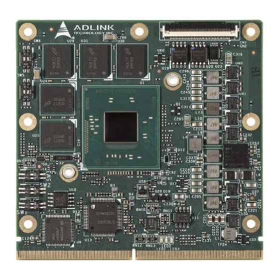
1.2 Major Components (ICs) Table 1-1 lists the major integrated circuits on the LEC-BT, including a brief description of each IC. Figure 1-2 shows the locations of the major ICs. Table 1-1: Major Integrated Circuit Descriptions and Functions Chip Type Mfg. - Page 9 LEC-BT Key: - CPU - Ethernet Controller - DDR3L SDRAM - DDR3L SDRAM - DDR3L SDRAM - DDR3L SDRAM (ECC) - DDR3L SDRAM Figure 1-2: Component Locations (Top Side) Key: - DDR3L SDRAM - DDR3L SDRAM - DDR3L SDRAM - DDR3L SDRAM...
-
Page 10: Connectors, Switches, And Leds
1.3 Connectors, Switches, and LEDs Table 1-2 describes the connectors, switches, and LEDs shown in Figure 1-4. Table 1-2: Module Connector Description Board Connector# Description Access GF1 – SMARC P-S Top/ 314-pin, MXM edge connector for routing Camera, Bottom Graphics, and I/O signals from the module to the baseboard 40-pin, DB40 connector for debug card SW1, SW2, SW3 –... - Page 11 LEC-BT Table 1-2: Module Connector Description (Continued) 4-pin dip switch for: • BIOS_SELECT (1=BIOS2 [blue LED blinks fast], 4=BIOS1 [default]) • WDT Disable (2=off [BMC switches to BIOS2 when BIOS1 not detected-default], 3=on [disables BIOS Detection Watchdog]) SW5 Switch Default Setting...
-
Page 12: Specifications
1.4 Specifications 1.4.1 Physical Specifications Table 1-3 lists the physical dimensions of the module. Table 1-3: Weight and Footprint Dimensions Overall height is measured from the upper board Item Dimension surface to the top of the highest permanent Weight 0.02 kg (0.05 lb) component (CN1 connector) on the upper board Height (overall) 2.50 mm (0.098 inches) -
Page 13: Electrical Specifications
LEC-BT 1.4.3 Electrical Specifications Table 1-4 specifies the electrical characteristics of the module. Table 1-4: Electrical Specifications Parameter Value Voltage Input Standard Fixed 5-Volt Supply (+4.75V DC min to +5.25V DC max) 3.0V, 2.0V to 3.3V (battery) Power States ... -
Page 14: Thermal/Cooling Requirements
1.4.6 Thermal/Cooling Requirements The LEC-BT is designed to operate at its maximum CPU speed and requires a thermal solution. ADLINK offers a heat spreader as one part of the cooling solution. CAUTION: The optional heat spreader plate requires another form of cooling, such as a fan. -
Page 15: Hardware
Hardware 2.1 CPU The LEC-BT product family offers multiple versions of the Intel Atom E3800 Series CPU (SoC): the E3805 (Dual Core, headless), the E3815 (Single Core), the E3826 (Dual Core), and the E3845 (Quad Core). E3800 CPUs feature the Intel 64 Architecture and are manufactured based on Intel’s 22-nanometer technology. -
Page 16: Interfaces
The main chips used in the LEC-BT may provide more features or options than are listed for the LEC-BT, but some of these features or options are not supported on the module and will not function as specified in the chip documentation. -
Page 17: Camera (Csi)
3.5 PCI Express (PCIe) The CPU features four PCIe x1 ports, and the LEC-BT module uses three of them for the PCIe interface and one of them for the Gigabit Ethernet interface. The PCIe interface supports the PCIe Base Specification 2.0 with a maximum signal rate of 5 GT/s and can be configured to sup- port PCIe edge cards or Express Cards. -
Page 18: I2C Bus
BMC or RTD2136 LVDS_DID 3.10 SPI The LEC-BT implements the SPI1 controller from the SoC (the SPI0 controller is not con- nected). The SPI1 controller connects to the SMARC connector at pins P54, P56, P57, and P58 (pin P55 is not connected), which support two SPI Flash devices on the module for BIOS stor- age. -
Page 19: Gpio
LEC-BT 3.15 GPIO The LEC-BT provides 12 GPIO signals from the PCA9535A GPIO expander on the module. The GPIO signals can be utilized for General Purpose IOs as well as camera reset, camera power, and HDA reset. Table 3-1: GPIO Default Settings... -
Page 20: Lpc Debug
3.17 LPC Debug A 40-pin, front flip, DB40 connector allows access to debug and update the BIOS, BMC, and OS code on the module. (Refer to “Debug (DB40)” on page 21.) 3.18 SMARC Interface Signals Table 3-3 provides the pin signals for the SMARC P-S connector. Refer to the SMARC specifica- tion at http://www.sget.org/standards/smarc.html for definitions of the SMARC signals. - Page 21 LEC-BT Table 3-3: SMARC P-S Connector (GF1) Signal Descriptions (Continued) GBE_LINK_ACT# (Link / Activity SDMMC_D0 (bidirectional, 8-bit data path; Indication LED Driven low on Link [10, may be used for 4- and 1-bit wide eMMC 100 or 1000 mbps] Blinks on Activity; able...
- Page 22 Table 3-3: SMARC P-S Connector (GF1) Signal Descriptions (Continued) SATA0_TX- (Differential SATA 0 transmit I2S2_LRCK (Left & Right audio data Pair; 0.1 uF 0402 capacitor on synchronization clock) module) I2S2_SDOUT (Digital audio output) SATA0_RX+ (Differential SATA 0 receive I2S2_SDIN (Digital audio input) data Pair;...
- Page 23 LEC-BT Table 3-3: SMARC P-S Connector (GF1) Signal Descriptions (Continued) USB2_EN_OC# (Pulled low by Module AFB_DIFF3- (maps to SATA_TX1_N on the OD driver to disable USB2 power. Pulled SOC) low by Carrier OD driver to indicate over- current situation. A pull-up shall be present on the Module to a 3.3V rail.
- Page 24 Table 3-3: SMARC P-S Connector (GF1) Signal Descriptions (Continued) PCIE_A_TX- (Differential PCIe Link A PCIE_B_TX- (Differential PCIe Link B transmit data pair 0. Series coupling transmit data pair 0. Series coupling caps capacitors are on the Module. 0.1 uF 0402 are on the Module Caps are 0402 package capacitor are on module) 0.1uF)
- Page 25 LEC-BT Table 3-3: SMARC P-S Connector (GF1) Signal Descriptions (Continued) P121 I2C_PM_CK (Power management I2C S122 Not connected bus clock) P122 I2C_PM_DAT(Power management I2C S123 Not connected bus data) P123 BOOT_SEL0# (Input straps determine the S124 Module boot device. Pulled up on Module.
- Page 26 Table 3-3: SMARC P-S Connector (GF1) Signal Descriptions (Continued) P144 Not connected S145 WDT_TIME_OUT# (Watchdog Timer Output) P145 Not connected S146 PCIE_WAKE (PCIe wake up interrupt to host – common to PCIe; links A, B, C – pulled up or terminated on Module) P146 Not connected S147...
-
Page 27: Debug (Db40)
LEC-BT Table 3-3: SMARC P-S Connector (GF1) Signal Descriptions (Continued) P154 VDD_IN (Module power input voltage - S155 FORCE_RECOV# (Low on this pin allows 3.0V min to 5.25V max) non-protected segments of Module boot device to be rewritten / restored from an external USB Host on Module USB0. - Page 28 Table 3-4: Debug Interface Signals (CN1) (Continued) 3V3_SMC1 LPC_AD0 LPC_AD1 LPC_AD2 LPC_AD3 LPC_FRAME# CLK33_LPC RST# BIOS_DIS0 GND2 LPC_3V3 SPI_BIOS_CLK SPI_BIOS_MOSI SPI_BIOS_MISO SPI_BIOS_CS1# SPI_BIOS_CS0# GND1 VCC_SPI_IN NOTE: The gray table cells denote ground. Interfaces...
-
Page 29: Utilities
Utilities 4.1 BIOS The LEC-BT features an AMI BIOS. The default settings provide a “ready to run” system, even without a BIOS setup backup battery. The BIOS is located in flash memory and can be easily updated with software under DOS. -
Page 30: Advanced Settings Screen
4.1.3 Advanced Settings screen The main screen of “Advanced Settings” provides configuration settings for CPU, Graphics, SATA, USB, SDIO, Network, Audio, PCI/PCIe, Devices, ACPI, Serial, Thermal, Security, Miscel- laneous, and SIO. Inappropriate values for any of the following advanced settings below may cause the system to malfunction. Utilities... - Page 31 LEC-BT Advanced > CPU Utilities...
- Page 32 Advanced > Graphics Advanced > SATA Utilities...
- Page 33 LEC-BT Advanced > USB Advanced > SDIO Utilities...
- Page 34 Advanced > Audio Advanced > PCI-PCIe Utilities...
- Page 35 LEC-BT Advanced > ACPI Advanced > Serial Utilities...
- Page 36 Advanced > Thermal Advanced > Security Utilities...
- Page 37 LEC-BT Advanced > Miscellaneous Advanced > SDIO Utilities...
-
Page 38: Security Screen
Security screen 4.1.5 Boot screen If more than one drive is attached to the LEC-BT, you can select from the first “Boot Configura- tion” screen the boot order in which the drives are scanned for a bootable OS image. Utilities... -
Page 39: Save & Exit Screen
LEC-BT 4.1.6 Save & Exit screen Utilities... -
Page 40: Sema Functions
Board Specific SEMA functions Voltages The BMC of the LEC-BT implements a Voltage Monitor and samples several Onboard Voltages. The Voltages can be read by calling the SEMA function, “Get Voltages”. The function returns a 16-bit value divided in Hi-Byte (MSB) and Lo-Byte (LSB). - Page 41 Use Main Current Function Main Current The BMC of the LEC-BT implements a Current Monitor. The current can be read by calling the SEMA function “Get Main Current”. The function returns four 16-bit values divided in Hi-Byte (MSB) and Lo-Byte (LSB). These four values represent the last four currents drawn by the board.
-
Page 42: Watchdog Timer
4.3 Watchdog Timer The LEC-BT features three separate Watchdog Timers. One of them is integrated in the SoC and two are provided by the BMC (managed by the SEMA). The SoC Watchdog can be configured in the BIOS or by programming the Watchdog registers. -
Page 43: Appendix A Technical Support
LEC-BT Appendix A Technical Support ADLINK Technology, Inc. provides a number of methods for contacting Technical Support listed in Table A-1 below. Requests for support through Ask an Expert are given the highest priorities, and usually will be addressed within one working day. - Page 44 +49 (0) 991 290 94 – 10 Fax: +49 (0) 991 290 94 - 29 Email: emea@adlinktech.com ADLINK Technology, Inc. (French Liaison Office) Address: 6 allée de Londres, Immeuble Ceylan 91940 Les Ulis, France Tel: +33 (0) 1 60 12 35 66...
- Page 45 84 Genting Lane #07-02A, Cityneon Design Centre Singapore 349584 Tel: +65-6844-2261 Fax: +65-6844-2263 Email: singapore@adlinktech.com ADLINK Technology Singapore Pte. Ltd. (Indian Liaison Office) Address: #50-56, First Floor, Spearhead Towers Margosa Main Road (between 16th/17th Cross) Malleswaram, Bangalore - 560 055, India Tel: +91-80-65605817, +91-80-42246107 Fax:...
Need help?
Do you have a question about the LEC-BT and is the answer not in the manual?
Questions and answers