Table of Contents
Advertisement
Quick Links
Advertisement
Table of Contents

Subscribe to Our Youtube Channel
Related Manuals for Xilinx ALINX AC6150


Summary of Contents for Xilinx ALINX AC6150
- Page 1 Xilinx ALINX Core Board AC6150 User Manual...
-
Page 2: Version Record
ALINX Xilinx Core Board AC6150 User Manual Version Record Version Date Release By Description Rev 1.0 2020-11-08 Rachel Zhou First Release www.alinx.com 2 / 21... -
Page 3: Table Of Contents
ALINX Xilinx Core Board AC6150 User Manual Table of Contents Version Record.......................2 Part 1: AC6150 core board.................. 4 Part 2: FPGA......................5 Part 2.1: JTAG Interface................6 Part 3: DDR3 DRAM..................... 7 Part 4: SPI Flash....................9 Part 5: Crystal oscillator on Core Board............11 Part 6: LED Light on Core Board..............12... -
Page 4: Part 1: Ac6150 Core Board
ALINX Xilinx Core Board AC6150 User Manual Part 1: AC6150 core board FPGA+ DDR3 core board is based on XILINX's SPARTAN6 series XC6SLX150-2FG484C. This chip develops a high-performance core board with high speed, high bandwidth and high capacity. It is suitable for video image processing and high-speed data acquisition. -
Page 5: Part 2: Fpga
Part 2: FPGA As mentioned above, the FPGA model we use is XC6SLX150-2FG484C, which belongs to Xilinx's SPARTAN6 series. The speed grade is 2, and the temperature grade is Commercial grade. This model is a FGG484 package with 484 pins. Xilinx SPARTAN6 FPGA naming rules as below Figure 2-1: The Specific Chip Model Definition of SPARTAN6 Series www.alinx.com... -
Page 6: Part 2.1: Jtag Interface
ALINX Xilinx Core Board AC6150 User Manual Figure 2-2: FPGA chip on the core board The main parameters of the FPGA chip XC7A100T are as follows Name Specific parameters Logic Cells 147,443 Slices 23038 CLB flip-flops 184,304 4,824 Block RAM(kb)... -
Page 7: Part 3: Ddr3 Dram
ALINX Xilinx Core Board AC6150 User Manual the core board. Users can connect the pin headers on the core board and connect the download and core JTAG ports with DuPont cable. To achieve core board program download and debug of the FPGA chip without the carrier board. - Page 8 ALINX Xilinx Core Board AC6150 User Manual In addition, the normal operation of DDR3 requires DDR3 address line and control line to provide termination voltage VTT and DDR3 chip reference voltage VREF, VTT and VREF voltage are both 0.75V, the following Figure 3-2 is the power part schematic.
-
Page 9: Part 4: Spi Flash
ALINX Xilinx Core Board AC6150 User Manual DDR3 is connected to the BANK3 of the FPGA. DDR3 Pin Assignment Pin Name FPGA Pin Pin Name FPGA Pin DDR3_A[0] DDR3_A[11] DDR3_A[1] DDR3_A[12] DDR3_A[2] DDR3_A[13] DDR3_A[3] DDR3_A[14] DDR3_A[4] DDR3_BA[0] DDR3_A[5] DDR3_BA[1] DDR3_A[6]... - Page 10 ALINX Xilinx Core Board AC6150 User Manual Due to the non-volatile nature of SPI FLASH, it can be used as a boot device for the system to store the boot image of the system. These images mainly include FPGA bit files, core application code and other user data files. The specific models and related parameters of SPI FLASH are shown in Table 4-1.
-
Page 11: Part 5: Crystal Oscillator On Core Board
ALINX Xilinx Core Board AC6150 User Manual SPI Flash pin assignments: Pin Name FPGA Pin SPI_CLK SPI_CSn SPI_DIN AB20 SPI_DOUT AA20 Part 5: Crystal oscillator on Core Board The core board carries a 50M active crystal oscillator and a 27M active crystal oscillator. -
Page 12: Part 6: Led Light On Core Board
ALINX Xilinx Core Board AC6150 User Manual Figure 5-2: Crystal oscillator on the Core Board Crystal oscillator Pin Assignment Input Clock FPGA Pin 50MHz AB13 27MHz Part 6: LED Light on Core Board There are 6 red LED lights on the AC6045 FPGA core board, one of which is the power indicator light (PWR), one is the configuration LED light (DONE), and four are the user LED light. - Page 13 ALINX Xilinx Core Board AC6150 User Manual Figure 6-2: Power Indicator and Configure Indicator on the Core Board The schematic diagram of the four user LED sections is shown below. In Figure 6-3, When the FPGA pin output is logic 0, the LED will be lit.
-
Page 14: Part 7: Ac6150 Power Supply
ALINX Xilinx Core Board AC6150 User Manual User LEDs Pin Assignment LED Name FPGA Pin LED0 LED1 LED2 LED3 Part 7: AC6150 Power Supply In order for FGPA to work properly, it is necessary to provide three power supplies for P3V3, P1V2 and VCCIO for the FPGA. P3V3 is for the VCCAUX of the FPGA, the voltage is 3.3V;... - Page 15 ALINX Xilinx Core Board AC6150 User Manual Figure 7-1:Power Supply on core board schematic www.alinx.com 15 / 21...
-
Page 16: Part 8: Power Interface On Core Board
ALINX Xilinx Core Board AC6150 User Manual Figure 7-2: Power Supply Circuit on the AC6150 FPGA Core Board Part 8: Power interface on Core Board In order to make the core board work normally, the FPGA expansion baord needs to provide a +5V power supply to the core board through the expansion ports. -
Page 17: Part 9: Expansion Ports
ALINX Xilinx Core Board AC6150 User Manual If you need to debug the core board separately, power the core board through the Mini USB port (J2) of the core board, the Mini USB cable is connected to the USB port of the computer. - Page 18 ALINX Xilinx Core Board AC6150 User Manual Figure 9-1: Expansion Ports P1 www.alinx.com 18 / 21...
- Page 19 ALINX Xilinx Core Board AC6150 User Manual Figure 9-2: Expansion Ports P2 www.alinx.com 19 / 21...
- Page 20 ALINX Xilinx Core Board AC6150 User Manual Figure 9-3: Expansion Ports P1&P2 on the Core Board www.alinx.com 20 / 21...
-
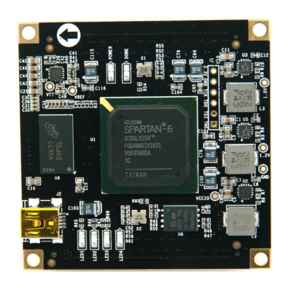
Page 21: Part 10: Structure Diagram
ALINX Xilinx Core Board AC6150 User Manual Part 10: Structure Diagram Figure 10-1: AC6150 FPGA Core board (Top view) Figure 10-2: AC6150 FPGA Core board (Rear view) www.alinx.com 21 / 21...
Need help?
Do you have a question about the ALINX AC6150 and is the answer not in the manual?
Questions and answers