Table of Contents
Advertisement
Quick Links
Advertisement
Table of Contents

Related Manuals for Terasic SoCKit


Summary of Contents for Terasic SoCKit
- Page 1 SoCKit User Manual www.terasic.com December 1, 2015...
-
Page 2: Table Of Contents
1.3 Getting Help ............................5 CHAPTER 2 INTRODUCTION OF THE SOCKIT BOARD ................. 6 2.1 Layout and Components ........................6 2.2 Block Diagram of the SoCKit Board ....................9 CHAPTER 3 USING THE SOCKIT BOARD ..................... 11 3.1 Board Setup Components ........................11 3.1.1 JTAG Chain and Setup Switches .................... - Page 3 CHAPTER 4 SOCKIT SYSTEM BUILDER ..................... 47 4.1 Introduction ............................47 4.2 General Design Flow .......................... 47 4.3 Using SoCKit System Builder ......................48 CHAPTER 5 EXAMPLES FOR FPGA ....................53 5.1 Audio Recording and Playing ......................53 5.2 A Karaoke Machine ..........................56 5.3 DDR3 SDRAM Test ...........................
- Page 4 CHAPTER 7 STEPS OF PROGRAMMING THE QUAD SERIAL CONFIGURATION DEVICE ....88 CHAPTER 8 APPENDIX .......................... 96 8.1 Revision History ..........................96 8.2 Copyright Statement ........................... 96 SoCKit User Manual www.terasic.com December 1, 2015...
-
Page 5: Sockit Development Kit
DDR3 memory, video and audio capabilities, Ethernet networking, and much more. In addition, an on-board HSMC connector with high-speed transceivers allows for an even greater array of hardware setups. By leveraging all of these capabilities, the SoCKit is the perfect solution for showcasing, evaluating, and prototyping the true potential of the Altera SoC. -
Page 6: Sockit System Cd
Ethernet Cable 12V DC power adapter The SoCKit System CD containing the SoCKit documentation and supporting materials, including the User Manual, System Builder, reference designs and device datasheets. User can download this System CD form the link : http:/sockit_support.terasic.com. -
Page 7: Introduction Of The Sockit Board
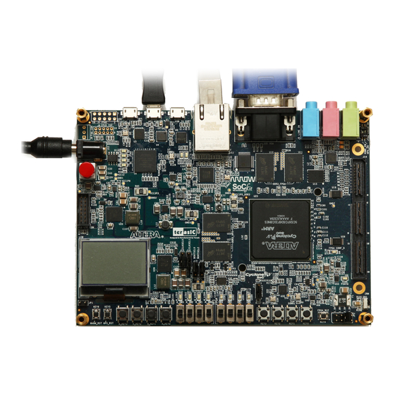
Chapter 2 Introduction of the SoCKit Board This chapter presents the features and design characteristics of the board. A photograph of the board is shown in Figure 2-1 Figure 2-2. It depicts the layout of the board and indicates the location of the connectors and key components. - Page 8 Cyclone V SoC 5CSXFC6D6F31 Device Dual-core ARM Cortex-A9 (HPS) 110K Programmable Logic Elements 5,140 Kbits embedded memory 6 Fractional PLLs 2 Hard Memory Controllers 3.125G Transceivers SoCKit User Manual www.terasic.com December 1, 2015...
- Page 9 8 User Keys (FPGA x4 ; HPS x 4) 8 User Switches (FPGA x4 ; HPS x 4) 8 User LEDs (FPGA x4 ; HPS x 4) 2 HPS Reset Buttons (HPS_RSET_n and HPS_WARM_RST_n) SoCKit User Manual www.terasic.com December 1, 2015...
-
Page 10: Block Diagram Of The Sockit Board
To provide maximum flexibility for the user, all connections are made through the Cyclone V SoC FPGA device. Thus, the user can configure the FPGA to implement any system design. SoCKit User Manual www.terasic.com December 1, 2015... - Page 11 Figure 2-3 Board Block Diagram SoCKit User Manual www.terasic.com December 1, 2015...
-
Page 12: Using The Sockit Board
JTAG chain, HSMC I/O voltage control, HPS boot source select, and others. This section will explain the settings and functions in detail. The SoCKit allows users to access the FPGA, HPS debug, or other JTAG chain devices via the on-board USB Blaster II. - Page 13 Figure 3-2 JTAG Chain and Setup Switches Table 3-1 SW4 JTAG Control DIP Switch Board Reference Signal Name Description Default On: Bypass HPS SW4.1 JTAG_HPS_EN Off: HPS In-chain SW4.2 JTAG_HSMC_EN On: Bypass HSMC SoCKit User Manual www.terasic.com December 1, 2015...
-
Page 14: Fpga Configuration Mode Switch
However, once the FPGA is in AS x4 mode, and after successfully configuring the FPGA via the EPCQ256, the SoCKit will be unable to boot Linux from the SD card or other devices. Please switch SW6 to another mode (e.g. MSEL[4:0] = 00001) to enable normal operations of Linux. -
Page 15: Hps Bootsel And Clksel Setting Headers
Figure 3-4) and CLKSEL jumpers (J15~J16, See Figure 3-5). Table 3-4 lists BOOTSEL and CLKSEL settings. Table 3-5 lists the settings for selecting a suitable boot source. Figure 3-4 HPS BOOTSEL Setting Headers SoCKit User Manual www.terasic.com December 1, 2015... - Page 16 1.8 V SD/MMC Flash memory(*1) 3.0 V SD/MMC Flash memory 1.8 V SPI or quad SPI Flash memory(*1) 3.0 V SPI or quad SPI Flash memory (*1) : Not supported on SoCKit board SoCKit User Manual www.terasic.com December 1, 2015...
-
Page 17: Hsmc Vccio Voltage Level Setting Header
On the SoCKit, the I/O standards of the FPGA/HSMC pins can be adjusted via JP2 (See Figure 3-6). Adjustable standards allow even more flexibility and selection of daughter cards or interconnect devices. The HSMC connector’s default standard is 2.5V. Users must ensure that the voltage standards for both the main board and daughter card are the same, or damage/incompatibility may occur. -
Page 18: Board Status Elements
The board equips two HPS reset circuits and one FPGA Device Clear button (See Figure 3-7). Table 3-8 shows the buttons references and its descriptions. Figure 3-8 shows the reset tree on the board. SoCKit User Manual www.terasic.com December 1, 2015... - Page 19 Warm reset to the HPS block. Active low input affects the KEY6 HPS_WARM_RST_n system reset domains which allows debugging to operate. This signal connects to the Cyclone V DEV_CLRn pin. When KEY4 FPGA_RESET_n this pin is driven low, all the device registers are. SoCKit User Manual www.terasic.com December 1, 2015...
-
Page 20: Programming The Quad-Serial Configuration Device
SFL solution Please refer to Chapter 6: Steps of Programming the Quad Serial Configuration Device for the basic programming instruction on the serial configuration device SoCKit User Manual www.terasic.com December 1, 2015... -
Page 21: Clock Circuits
(SW6) to ASx4 mode. Figure 3-10 is a diagram showing the default frequencies of all of the external clocks going to the Cyclone V SoC FPGA. Figure 3-10 Block diagram of the clock distribution SoCKit User Manual www.terasic.com December 1, 2015... -
Page 22: Interface On Fpga
Figure 3-11 Connections between the push-button and Cyclone V SoC FPGA Pushbutton depressed Pushbutton released Before Debouncing Schmitt Trigger Debounced Figure 3-12 Switch debouncing SoCKit User Manual www.terasic.com December 1, 2015... - Page 23 LED on, and driving the pin low turns it off. Figure 3-14 shows the connections between LEDs and Cyclone V SoC FPGA. Table 3-9, Table 3-10 Table 3-11 list the pin assignments of these user interfaces. SoCKit User Manual www.terasic.com December 1, 2015...
- Page 24 Table 3-11 Pin Assignments for LEDs Signal Name FPGA Pin No. Description I/O Standard LED[0] PIN_AF10 LED [0] 3.3V LED[1] PIN_AD10 LED [1] 3.3V LED[2] PIN_AE11 LED [2] 3.3V LED[3] PIN_AD7 LED [3] 3.3V SoCKit User Manual www.terasic.com December 1, 2015...
-
Page 25: Hsmc Connector
Table 3-13 Pin Assignments for HSMC connector Signal Name FPGA Pin No. Description I/O Standard HSMC_CLK_IN0 PIN_J14 Dedicated clock input Depend on JP2 HSMC_CLKIN_n1 PIN_AB27 LVDS RX or CMOS I/O or Depend on JP2 differential clock input SoCKit User Manual www.terasic.com December 1, 2015... - Page 26 1.5-V PCML HSMC_GXB_RX_n[5] PIN_R1 Transceiver RX bit 5n 1.5-V PCML HSMC_GXB_RX_n[6] PIN_N1 Transceiver RX bit 6n 1.5-V PCML HSMC_GXB_RX_n[7] PIN_J1 Transceiver RX bit 7n 1.5-V PCML HSMC_GXB_TX_n[0] PIN_AD3 Transceiver TX bit 0n 1.5-V PCML SoCKit User Manual www.terasic.com December 1, 2015...
- Page 27 LVDS TX bit 1n or CMOS I/O Depend on JP2 HSMC_TX _n[2] PIN_F6 LVDS TX bit 2n or CMOS I/O Depend on JP2 HSMC_TX _n[3] PIN_C5 LVDS TX bit 3n or CMOS I/O Depend on JP2 SoCKit User Manual www.terasic.com December 1, 2015...
-
Page 28: Audio Codec
Figure 3-16. Detailed information for using the SSM2603 codec is available in its datasheet, which can be found on the manufacturer’s website, or in the Datasheets\Audio CODEC folder on the SoCKit System CD SoCKit User Manual www.terasic.com December 1, 2015... -
Page 29: Vga
10-bit high-speed video DAC (only the higher 8-bits are used) is used to produce the analog data signals (red, green, and blue). It could support the SXGA standard (1280*1024) with a bandwidth of 100MHz. Figure 3-17 gives the associated schematic SoCKit User Manual www.terasic.com December 1, 2015... - Page 30 Detailed information for using the ADV7123 video DAC is available in its datasheet, which can be found on the manufacturer’s website, or in the Datasheets\VIDEO DAC folder on the SoCKit System CD. The pin assignments between the Cyclone V SoC FPGA and the ADV7123 are listed in...
- Page 31 Table 3-16 VGA Vertical Timing Specification VGA mode Vertical Timing Spec Configuration Resolution(HxV) a(lines) b(lines) c(lines) d(lines) Pixel clock(MHz) VGA(60Hz) 640x480 VGA(85Hz) 640x480 SVGA(60Hz) 800x600 SVGA(75Hz) 800x600 SVGA(85Hz) 800x600 XGA(60Hz) 1024x768 XGA(70Hz) 1024x768 XGA(85Hz) 1024x768 1280x1024(60Hz) 1280x1024 1024 SoCKit User Manual www.terasic.com December 1, 2015...
-
Page 32: Ir Receiver
IR Receiver The board provides an infrared remote-control receiver module (model: IRM-V5XX/TR1), whose datasheet is offered in the Datasheets\IR_Receiver folder on SoCKit System CD. The accompanied remote controller with an encoding chip of uPD6121G is very suitable of generating expected infrared signals. -
Page 33: Ddr3 Memory On Fpga
300MHz if the hard external memory interface if not enabled. Figure 3-20 shows the connections between the DDR3 and Cyclone V SoC FPGA. Table 3-19 shows the DDR3 interface pin assignments. Figure 3-20 Connections between FPGA and DDR3 SoCKit User Manual www.terasic.com December 1, 2015... - Page 34 DDR3 Data[8] SSTL-15 Class I DDR3_DQ[9] PIN_AJ17 DDR3 Data[9] SSTL-15 Class I DDR3_DQ[10] PIN_AG18 DDR3 Data[10] SSTL-15 Class I DDR3_DQ[11] PIN_AK19 DDR3 Data[11] SSTL-15 Class I DDR3_DQ[12] PIN_AG20 DDR3 Data[12] SSTL-15 Class I SoCKit User Manual www.terasic.com December 1, 2015...
- Page 35 PIN_AH8 DDR3 Row Address Strobe SSTL-15 Class I DDR3_RESET_n PIN_AK21 DDR3 Reset SSTL-15 Class I DDR3_WE_n PIN_AJ6 DDR3 Write Enable SSTL-15 Class I External reference ball for 1.5V DDR3_RZQ PIN_AG17 output drive calibration SoCKit User Manual www.terasic.com December 1, 2015...
-
Page 36: Temperature Sensor
0.03125°C. The interface between sensor and FPGA is SPI serial interface. Detailed information for using the sensor is available in its datasheet, which can be found on the manufacturer’s website, or in the Datasheets\TEMP_Sensor folder on the SoCKit System CD. -
Page 37: User Push-Buttons, Switches And Led On Hps
Gigabit Ethernet PHY and Cyclone V SoC FPGA. The associated pin assignments are listed in Table 3-22. For detailed information on how to use the KSZ9021RN refers to its datasheet and application notes, which are available on the manufacturer’s website. SoCKit User Manual www.terasic.com December 1, 2015... - Page 38 Table 3-23, which can display the current status of the Ethernet. For example once the green LED lights on , the board has been connected to Giga bit Ethernet. SoCKit User Manual www.terasic.com December 1, 2015...
-
Page 39: Uart
FT232R chip and connects to the host using a Mini-USB (B) connector. For detailed information on how to use the transceiver, please refer to the datasheet, which is available on the manufacturer’s website, or in the Datasheets\FT232 folder on the SoCKit System CD. Figure 3-23... -
Page 40: Ddr3 Memory On Hps
SSTL-15 Class I HPS_DDR3_DQ[2] PIN_H30 HPS DDR3 Data[2] SSTL-15 Class I HPS_DDR3_DQ[3] PIN_G28 HPS DDR3 Data[3] SSTL-15 Class I HPS_DDR3_DQ[4] PIN_L25 HPS DDR3 Data[4] SSTL-15 Class I HPS_DDR3_DQ[5] PIN_L24 HPS DDR3 Data[5] SSTL-15 Class I SoCKit User Manual www.terasic.com December 1, 2015... -
Page 41: Qspi Flash
HPS DDR3 Write Enable SSTL-15 Class I HPS_DDR3_RZQ PIN_D27 External reference ball for 1.5 V output drive calibration The board supports a 512M-bit serial NOR flash device for non-volatile storage of HPS boot code, SoCKit User Manual www.terasic.com December 1, 2015... -
Page 42: Micro Sd
The board supports Micro SD card interface using x4 data lines. And it may contain secondary boot code for HPS. Figure 3-25 shows the related signals. Finally, Table 3-27 lists all the associated pins for interfacing HPS respectively. SoCKit User Manual www.terasic.com December 1, 2015... -
Page 43: Usb 2.0 Otg Phy
Host mode, the interface will supply the power to the device through the Mini-USB interface. Figure 3-26 shows the schematic diagram of the USB circuitry; the pin assignments for the associated interface are listed in Table 3-28. SoCKit User Manual www.terasic.com December 1, 2015... -
Page 44: G-Sensor
G-Sensor device is 0xA6/0xA7. For more detailed information of better using this chip, please refer to its datasheet which is available on manufacturer’s website or under the Datasheet folder of the SoCKit System CD. Figure 3-27 shows the connections between ADXL345 and HPS. -
Page 45: 128X64 Dots Lcd
The board equips an LCD Module with 128x64 dots for display capabilities. The LCD module uses serial peripheral interface to connect with the HPS. To use the LCD module, please refer to the datasheet folder in SoCKit System CD. Figure 3-28 shows the connections between the HPS and LCD module. -
Page 46: Ltc Connector
Linear Technology board aren’t in use. Connections between the LTC connector and the HPS are shown in Figure 3-29, and the functions of the 14 pins is listed in Table 3-31. SoCKit User Manual www.terasic.com December 1, 2015... - Page 47 HPS I2C Data (share bus with G-Sensor) 3.3V HPS_SPIM_CLK PIN_A23 SPI Clock 3.3V HPS_SPIM_MISO PIN_B23 SPI Master Input/Slave Output 3.3V HPS_SPIM_MOSI PIN_C22 SPI Master Output /Slave Input 3.3V HPS_SPIM_SS PIN_H20 SPI Slave Select 3.3V SoCKit User Manual www.terasic.com December 1, 2015...
-
Page 48: Sockit System Builder
This chapter describes how users can create a custom design project on the board by using the SoCKit Software Tool – SoCKit System Builder. The SoCKit System Builder is a Windows-based software utility, designed to assist users to create a Quartus II project for the board within minutes. The generated Quartus II project files include: ... -
Page 49: Using Sockit System Builder
JTAG interface. Figure 4-1 The general design flow of building a design This section provides the detailed procedures on how the SoCKit System Builder is used. Install and launch the SoCKit System Builder The SoCKit System Builder is located in the directory: “Tools\SOC_Kit_system_builder”... - Page 50 Figure 4-2 The SoCKit System Builder window Input Project Name Input project name as show in Figure 4-3. Project Name: Type in an appropriate name here, it will automatically be assigned as the name of your top-level design entity.
- Page 51 If the component is enabled, the SoCKit System Builder will automatically generate the associated pin assignments including the pin name, pin location, pin direction, and I/O standard.
- Page 52 The “Prefix Name” is an optional feature that denotes the pin name of the daughter card assigned in your design. Users may leave this field empty. Project Setting Management The SoCKit System Builder also provides functions to restore default setting, loading a setting, and saving users’ board configuration file shown in Figure 4-6.
- Page 53 Figure 4-6 Project Settings Project Generation When users press the Generate button, the SoCKit System Builder will generate the corresponding Quartus II files and documents as listed in the Table 4-1: Table 4-1 The files generated by SoCKit System Builder...
-
Page 54: Examples For Fpga
– otherwise, the Nios II software will not work. Note Quartus II v13 is required for all SoCKit demonstrations to support Cyclone V SoC device. This demonstration shows how to implement an audio recorder and player using the SoCKit board with the built-in Audio CODEC chip. - Page 55 Master Mode. The audio interface is configured as I2S and 16-bit mode. 18.432MHz clock generated by the PLL is connected to the MCLK/XTI pin of the audio chip through the AUDIO Controller. SoCKit User Manual www.terasic.com December 1, 2015...
- Page 56 Bit stream used: SoCKit _Audio.sof Software Project directory: SoCKit _Audio\software Connect an Audio Source to the LINE-IN port of the SoCKit board. Connect a Microphone to MIC-IN port on the SoCKit board. Connect a speaker or headset to LINE-OUT port on the SoCKit board.
-
Page 57: A Karaoke Machine
(2). Recording process will stop if audio buffer is full. (3). Playing process will stop if audio data is played completely. This demonstration uses the microphone-in, line-in, and line-out ports on the SOCKIT board to create a Karaoke Machine application. The SSM2603 audio CODEC is configured in the master mode, with which the audio CODEC generates AD/DA serial bit clock (BCK) and the left/right channel clock (LRCK) automatically. - Page 58 Project directory: SOCKIT_i2sound Bit stream used: SOCKIT_i2sound.sof Connect a microphone to the microphone-in port (pink color) on the SOCKIT board Connect the audio output of a music-player, such as an MP3 player or computer, to the line-in port (blue color) on the SOCKIT board ...
- Page 59 Figure 5-4 Setup for the Karaoke Machine SoCKit User Manual www.terasic.com December 1, 2015...
-
Page 60: Ddr3 Sdram Test
This demonstration presents a memory test function on the bank of DDR3-SDRAM on the SoCKit board. The memory size of the DDR3 SDRAM bank is 1GB. Function Block Diagram Figure 5-5 shows the function block diagram of this demonstration. The controller uses 50 MHz as a reference clock, generates one 300 MHz clock as memory clock, and generates one half-rate system clock 150MHz for the controller itself. - Page 61 Demonstration Setup Make sure Quartus II is installed on your PC. Connect the USB cable to the USB Blaster II connector (J2) on the SoCKit board and host PC. Power on the SoCKit board. Execute the demo batch file “SoCKit_DDR3_RTL_Test.bat” under the batch file folder, SoCKit_DDR3_RTL_Test \demo_batch.
-
Page 62: Ddr3 Sdram Test By Nios Ii
1 GB of SDRAM. Then, it calls Nios II system function, alt_dache_flush_all, to make sure all data has been written to SDRAM. Finally, it reads data from SDRAM for data SoCKit User Manual www.terasic.com December 1, 2015... - Page 63 Batch File for USB-Blaster (II) : SoCKit_DDR3_Nios_Test.bat, SoCKit_DDR3_Nios_Test_bashrc FPGA Configure File : SoCKit_DDR3_Nios_Test.sof Nios II Program: SoCKit_DDR3_Nios_Test.elf Demonstration Setup Make sure Quartus II and Nios II are installed on your PC. SoCKit User Manual www.terasic.com December 1, 2015...
-
Page 64: Ir Receiver Demonstration
Power on the SoCKit board. Use USB cable to connect PC and the SoCKit board (J2) and install USB Blaster driver if necessary. Execute the demo batch file “SoCKit_DDR3_Nios_Test.bat” for USB-Blaster II under the batch file folder, SoCKit_DDR3_Nios_Test\demo_batch ... - Page 65 Finally, the key code information will be displayed in nios2-terminal. Figure 5-9 shows the block diagram of the design. Figure 5-8 Terasic Remote controller Table 5-4 Key code information for each Key on remote controller Key Code Key Code...
- Page 66 1 bit end code represents the end of the frame. Inv Key Code Code Lead Code 1bit Custom Code 16bits Key Code 8bits 8bits 1bit Figure 5-10 The transmitting frame of the IR remote controller SoCKit User Manual www.terasic.com December 1, 2015...
- Page 67 After the IR receiver on SoCKit receives this frame, it will directly transmit that to FPGA. In this demo, the IP of IR receiver controller is implemented in the FPGA. As Figure 5-11 shows, it includes Code Detector, State Machine, and Shift Register. First, the IR receiver demodulates the signal input to Code Detector block.
- Page 68 Make sure Quartus II and Nios II are installed on your PC. Power on the SoCKit board. Connect USB Blaster to the SoCKit board and install USB Blaster driver if necessary. Execute the demo batch file “SoCKit _IR.bat” under the batch file folder, SoCKit _IR \demo_batch.
-
Page 69: Temperature Demonstration
The ambient temperature information, which is collected by a built-in temperature sensor on the SoCKit board, can be converted into digital data by a 13-bit A/D converter. The generated digital data will be stored into the Temperature Value Register. - Page 70 Nios II Workspace: SoCKit_TEMP\Software Demo Batch File Folder: SoCKit_TEMP\demo_batch The demo batch file includes the following files: Batch File: SoCKit_TEMP.bat, SoCKit_TEMP_bashrc FPGA Configure File : SoCKit_TEMP.sof Nios II Program: SoCKit _TEMP.elf SoCKit User Manual www.terasic.com December 1, 2015...
- Page 71 Make sure Quartus II and Nios II are installed on your PC. Power on the SoCKit board. Connect USB Blaster to the SoCKit board and install USB Blaster driver II if necessary. Execute the demo batch file “SoCKit _TEMP.bat” under the batch file folder, SoCKit _TEMP \demo_batch.
-
Page 72: Examples For Hps Soc
LED/button/switch, I2C interfaced G-sensor, and SPI interfaced graphic LCD. All of the associated files can be found in the Demonstrations/SOC folder in the SoCKit System CD. Installation of the Demonstrations To install the demonstrations on your computer: Copy the directory Demonstrations into a local directory of your choice. - Page 73 Use the "cd" command to change the current directory to where the Hello World project is located. Then type "make" to build the project. The executable file "my_first_hps" will be generated after the compiling process is finished. The "clean all" command can be used to remove all temporary files. SoCKit User Manual www.terasic.com December 1, 2015...
-
Page 74: Users Led, Switch And Button
Make sure MSEL[4:0] = 00001 Connect USB cable to the USB-to-UART connector (J4) on the SoCKit board and host PC. Make sure the demo file "my_first_hps" is copied into the SD card under the "/home/root" folder in Linux. - Page 75 GPIO Interface. GPIO[28..0] is controlled by GPIO0 controller and GPIO[57..29] is controlled by GPIO1 controller. GPIO[70..58] and input-only GPI[13..0] are controlled by GPIO2 controller. Figure 6-2 Block Diagram of GPIO Interface SoCKit User Manual www.terasic.com December 1, 2015...
- Page 76 Registers of GPIO1 controller are mapped to the base address 0xFF208000 with 4KB size, and registers of GPIO2 controller are mapped to the base address 0xFF20A000 with 4KB size, as shown Figure 6-3. SoCKit User Manual www.terasic.com December 1, 2015...
- Page 77 To use the above API to access register of GPIO controller, the program must include the following header files. #include <stdio.h> #include <unistd.h> #include <fcntl.h> #include <sys/mman.h> #include "hwlib.h" #include "socal/socal.h" #include "socal/hps.h" #include "socal/alt_gpio.h" SoCKit User Manual www.terasic.com December 1, 2015...
- Page 78 LED Control Figure 6-4 shows the HPS users LED pin assignment for the SoCKit board. The LED0, LED1, LED2, and LED3 are connected to HPS_GPIO53, HPS_GPIO54, HPS_GPIO55, and HPS_GPIO56, which are controlled by the GPIO1 controller, which also controls HPS_GPIO29 ~ HPS_GPIO57.
- Page 79 Switches and Keys Control Figure 6-6 shows the pin assignment of HPS users key and switch for the SoCKit board. The controller pin HPS_GPI4 ~ HPS_GPI11 are controlled by the GPIO2 controller. It is not necessary to configure the direction of these pins before using because they are input-only. The status of switches and keys can be queried by reading the gpio_ext_porta register in the GPIO2 controller.
- Page 80 GPIO2 controller, respectively. Figure 6-7 gpio_swpport_ddr Register in the GPIO1 Controller In the demo code, the following bit mask is defined to check the input status of switches and keys. SoCKit User Manual www.terasic.com December 1, 2015...
- Page 81 Insert the booting micro SD card into the SoCKit board. Power on the SoCKit board. Launch PuTTY to connect to the UART port of SoCKit board and type "root" to login Altera Yocto Linux. In the UART terminal of PuTTY, execute "./hps_pio" to start the program.
-
Page 82: I2C Interfaced G-Sensor
Function Block Diagram Figure 6-8 hows the function block diagram of this demonstration. The G-sensor on the SoCKit board is connected to the I2C1 controller in HPS. The G-Sensor I2C 7-bit device address is 0x53. The system I2C bus driver is used to access the register files in the G-sensor. The G-sensor interrupt signal is connected to the PIO controller. - Page 83 G-sensor Control The ADI ADXL345 provides I2C and SPI interfaces. I2C interface is used by setting the CS pin to high on this SoCKit board. The ADI ADXL345 G-sensor provides user-selectable resolution up to 13-bit ± 16g. The resolution can be configured through the DATA_FORAMT(0x31) register. In the demonstration, we configure the data format as: ...
- Page 84 Insert the booting micro sdcard into the SoCKit board. Power on the SoCKit board. Launch PuTTY to connect to the UART port of SoCKit borad and type "root" to login Yocto Linux. In the UART terminal of PuTTY,, execute "./gsensor" to start the gsensor polling.
-
Page 85: Spi Interfaced Graphic Lcd
Figure 6-11 hows the function block diagram of this demonstration. The LTC is connected to the SPIM1, GPIO1, and GPIO2 controllers in HPS on this SoCKit board. The built-in virtual memory-mapped device driver in the system is used to access the registers in the HPS SPIM and GPIO controllers. - Page 86 The main program main.c calls "LCDHW_Init" to initialize the SPIM1 and GPIO controllers, which are used to control the LCD. It then calls "LCDHW_BackLight" to turn on the backlight of LCD. "LCD_Init" is called to initialize LCD configuration. Finally, the APIs in lcd_graphic.c are SoCKit User Manual www.terasic.com December 1, 2015...
- Page 87 Power on the SoCKit board. Launch PuTTY to connect to the UART port of SoCKit board and type "root" to login Yocto Linux. In the UART terminal of PuTTY, type "./hps_lcd" to start the LCD demo, as shown in Figure 6-13.
- Page 88 Users should see the LCD displayed as shown in Figure 6-14. Figure 6-14 LCD display for the LCD Demonstration SoCKit User Manual www.terasic.com December 1, 2015...
- Page 89 To do this, adjust the configuration mode switch (SW6) to let MSEL[4..0] to be set as “10010”. Convert. SOF File to .JIC file Choose Convert Programming Files on Quartus window (File menu), See Figure 7-1. SoCKit User Manual www.terasic.com December 1, 2015...
- Page 90 In the Mode field, choose Active Serial X4. In the File name field, browse to the target directory and specify an output file name. Highlight the SOF data in the Input files to convert section. See Figure 7-2 SoCKit User Manual www.terasic.com December 1, 2015...
- Page 91 Select the SOF that you want to convert to a JIC file. Click Open. 10. Highlight the Flash Loader and click Add Device. See Figure 7-3. 11. Click OK. The Select Devices page displays. SoCKit User Manual www.terasic.com December 1, 2015...
- Page 92 Figure 7-3. Highlight Flash Loader Select the targeted FPGA that you are using to program the serial configuration device. See Figure 7-4 Click OK. The Convert Programming Files page displays. See Figure 7-5 Click Generate SoCKit User Manual www.terasic.com December 1, 2015...
- Page 93 Write JIC File into Quad Serial Configuration Device To program the serial configuration device with the JIC file that you just created, add the file to the Quartus II Programmer window and follow the steps: SoCKit User Manual www.terasic.com December 1, 2015...
- Page 94 Click Auto Detect and choose the device, Figure 7-6. iii. Click the FPGA device and right click mouse, click Change File and select .jic file for FPGA. Figure 7-7. Figure 7-6. Choose device Figure 7-7. Add .jic file SoCKit User Manual www.terasic.com December 1, 2015...
- Page 95 Choose Programmer (Tools menu), and the Chain.cdf window appears. Click Auto Detect, choose the device. Click the FPGA device, right click mouse and click Change File. Then select .jic file for FPGA (See Figure 7-9 SoCKit User Manual www.terasic.com December 1, 2015...
- Page 96 Figure 7-9 Erasing setting in Quartus II programmer window Click Start to erase the serial configuration device SoCKit User Manual www.terasic.com December 1, 2015...
-
Page 97: Chapter 8 Appendix
V0.2 Add CH5 and CH6 V0.3 Modify CH3 V0.4 Add CH6 HPS V1.0 Modify CH 7 V2.0 Modify Usb Connector, QSPI Flash and CH7 Copyright © 2015 Terasic Technologies Inc. All rights reserved. SoCKit User Manual www.terasic.com December 1, 2015...
Need help?
Do you have a question about the SoCKit and is the answer not in the manual?
Questions and answers