Table of Contents
Advertisement
Quick Links
Advertisement
Table of Contents

Related Manuals for Terasic DE5-Net


Summary of Contents for Terasic DE5-Net
- Page 1 DE5-Net User Manual www.terasic.com June 20, 2018...
-
Page 2: Table Of Contents
......................58 LASH ROGRAMMING WITH SERS ESIGN 4.4 R ..........................60 ESTORE ACTORY ETTINGS PROGRAMMABLE OSCILLATOR CHAPTER 5 ....................62 5.1 O ................................62 VERVIEW 5.2 S 570 E RTL ............................66 XAMPLE BY DE5-Net User Manual www.terasic.com June 20, 2018... - Page 3 – DDR3 ........................105 7.4 PCI EFERENCE ESIGN TRANSCEIVER VERIFICATION CHAPTER 8 ....................112 8.1 T ................................112 8.2 L ............................. 112 OOPBACK IXTURE 8.3 T ................................114 ESTING ADDITIONAL INFORMATION ........................... 116 DE5-Net User Manual www.terasic.com June 20, 2018...
-
Page 4: Chapter 1 Overview
The Stratix® V GX FPGA features integrated transceivers that transfer at a maximum of 12.5 Gbps, allowing the DE5-Net to be fully compliant with version 3.0 of the PCI Express standard, as well as allowing an ultra low-latency, straight connections to four external 10G SFP+ modules. Not relying on an external PHY will accelerate mainstream development of network applications enabling customers to deploy designs for a broad range of high-speed connectivity applications. -
Page 5: Key Features
The following hardware is implemented on the DE5-Net board: FPGA Altera Stratix® V GX FPGA (5SGXEA7N2F45C2) FPGA Configuration On-Board USB Blaster II or JTAG header for FPGA programming Fast passive parallel (FPPx32) configuration via MAX II CPLD and flash memory ... -
Page 6: Block Diagram
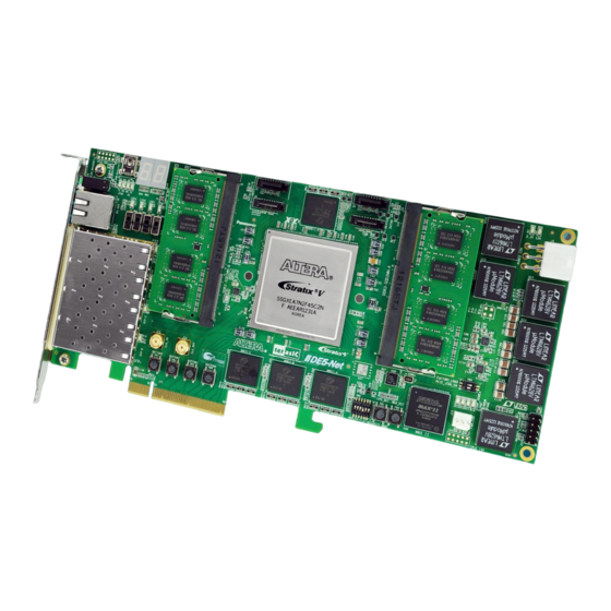
PCI Express full-height and 3/4-length F igure 1-1 shows the block diagram of the DE5-Net board. To provide maximum flexibility for the 9 4 H 9 4 H users, all key components are connected with the Stratix V GX FPGA device. Thus, users can configure the FPGA to implement any system design. - Page 7 Figure 1-1 Block diagram of the DE5-Net board Below is more detailed information regarding the blocks in Figure 1-1. Stratix V GX FPGA 5SGXEA7N2F45C2 622,000 logic elements (LEs) 50-Mbits embedded memory 48 transceivers (12.5Gbps) 512 18-bit x 18-bit multipliers ...
- Page 8 50MHz oscillator Programming PLL providing clock for 10G SFP+ transceiver Programming PLL providing clock for SATA or 1G SFP+ transceiver Four Serial ATA ports SATA 3.0 standard at 6Gbps signaling rate DE5-Net User Manual www.terasic.com June 20, 2018...
- Page 9 Support for PCIe Gen1/2/3 Edge connector for PC motherboard with x8 or x16 PCI Express slot Power Source PCI Express 6-pin DC 12V power PCI Express edge connector power DE5-Net User Manual www.terasic.com June 20, 2018...
-
Page 10: Chapter 2 Board Components
This chapter introduces all the important components on the DE5-Net. Figure 2-1 is the top and bottom view of the DE5-Net development board. It depicts the layout of the board and indicates the location of the connectors and key components. Users can refer to this figure for relative location of the connectors and key components. -
Page 11: Configuration , Status And Setup
Launch Quartus Prime programmer and make sure the USB-Blaster II is detected. In Quartus Prime Programmer, add the configuration bit stream file (.sof), check the associated “Program/Configure” item, and click “Start” to start FPGA programming. DE5-Net User Manual www.terasic.com June 20, 2018... - Page 12 SW7.1 PCIE_PRSNT2n_x1 Off: Disable x1 presence detect On : Enable x4 presence detect SW7.2 PCIE_PRSNT2n_x4 Off: Disable x4 presence detect On : Enable x8 presence detect SW7.3 PCIE_PRSNT2n_x8 Off: Disable x8 presence detect DE5-Net User Manual www.terasic.com June 20, 2018...
- Page 13 Setting Position 2 of SW5 to high (right) specifies the default factory image to be loaded, as shown Figure 2-4. Setting Position 2 of SW5 to low (left) specifies the DE5-Net to load a user-defined image, as shown in Figure 2-5.
-
Page 14: General User Input /Output
Stratix V GX device pin numbers. Table 2-3 Push-button Pin Assignments, Schematic Signal Names, and Functions Board Schematic Stratix V GX Description Reference Signal Name Standard Pin Number DE5-Net User Manual www.terasic.com June 20, 2018... - Page 15 Table 2-4 Slide Switch Pin Assignments, Schematic Signal Names, and Functions Board Schematic Stratix V GX Description Reference Signal Name Standard Pin Number High logic level when SW in the UPPER 1.8-V PIN_B25 position. 1.8-V PIN_A25 1.8-V PIN_B23 DE5-Net User Manual www.terasic.com June 20, 2018...
- Page 16 Each segment in a display is identified by an index listed from 0 to 6 with the positions given in Figure 2-8. In addition, the decimal point is identified as DP. Table 2-6 shows the mapping of the FPGA pin assignments to the 7-segment displays. DE5-Net User Manual www.terasic.com June 20, 2018...
- Page 17 1.5-V PIN_G16 logic 1 on the I/O port turns the 7-segment signal HEX1 HEX1_D2 1.5-V PIN_F16 OFF. HEX1 HEX1_D3 1.5-V PIN_A7 HEX1 HEX1_D4 1.5-V PIN_B7 HEX1 HEX1_D5 1.5-V PIN_C9 HEX1 HEX1_D6 1.5-V PIN_D10 DE5-Net User Manual www.terasic.com June 20, 2018...
-
Page 18: Temperature Sensor And Fan Control
Negative pin of temperature diode in TEMPDIODEn 1.8-V PIN_P7 Stratix V TEMP_CLK SMBus clock 2.5-V PIN_D21 TEMP_DATAT SMBus data 2.5-V PIN_D20 TEMP_OVERT_n SMBus alert (interrupt) 2.5-V PIN_C22 TEMP_INT_n SMBus alert (interrupt) 2.5-V PIN_C21 FAN_CTRL Fan control 2.5-V PIN_AR32 DE5-Net User Manual www.terasic.com June 20, 2018... -
Page 19: Clock Circuit
SATA reference clocks respectively. The Si570 programmable clock generator is programmed via an I2C serial interface to generate the 10G Ethernet SFP+ reference clock. Two SMA connectors provide external clock input and clock output respectively. DE5-Net User Manual www.terasic.com June 20, 2018... - Page 20 PIN_AV34 Clock Output Defined SFP_REFCLK _p 100.0 MHz LVDS PIN_AK7 10G SFP+ SFP1G_REFCLK_p 125.0 MHz LVDS PIN_AH6 1G SFP+ SATA_HOST_REFCLK_p 125.0 MHz LVDS PIN_V6 SATA HOST SATA_DEVICE_REFCLK_p 125.0 MHz LVDS PIN_V39 SATA DEVICE DE5-Net User Manual www.terasic.com June 20, 2018...
-
Page 21: Serial Port
Figure 2-11 shows the RS-422 block diagram of the development board. The full-duplex LTC2855 is used to translate the RS-422 signal, and the RJ45 is used as an external connector for the RS-422 signal. DE5-Net User Manual www.terasic.com June 20, 2018... -
Page 22: Flash Memory
Internal Termination Resistance Enable. A high input will connect a RS422_TE PIN_AF16 termination resistor (120Ω typical) between pins A and B. The development board has two 1Gb CFI-compatible synchronous flash devices for non-volatile DE5-Net User Manual www.terasic.com June 20, 2018... - Page 23 Address bus 2.5-V PIN_AJ32 FSM_A6 Address bus 2.5-V PIN_AG33 FSM_A7 Address bus 2.5-V PIN_AL30 FSM_A8 Address bus 2.5-V PIN_AK33 FSM_A9 Address bus 2.5-V PIN_AJ33 FSM_A10 Address bus 2.5-V PIN_AN30 FSM_A11 Address bus 2.5-V PIN_AH33 DE5-Net User Manual www.terasic.com June 20, 2018...
- Page 24 Data bus 2.5-V PIN_AW32 FSM_D20 Data bus 2.5-V PIN_BD32 FSM_D21 Data bus 2.5-V PIN_AY31 FSM_D22 Data bus 2.5-V PIN_BA30 FSM_D23 Data bus 2.5-V PIN_BB30 FSM_D24 Data bus 2.5-V PIN_AM29 FSM_D25 Data bus 2.5-V PIN_AR29 DE5-Net User Manual www.terasic.com June 20, 2018...
-
Page 25: Ddr3 So-Dimm
Using differential DQS signaling for the DDR3 SDRAM interfaces, it is capable of running at up to 800MHz memory clock for a maximum theoretical bandwidth up to 95.4Gbps. Figure 2-13 shows the connections between the DDR3 SDRAM SO-DIMMs and Stratix V GX FPGA. DE5-Net User Manual www.terasic.com June 20, 2018... - Page 26 Data [5] SSTL-15 Class I PIN_D35 DDR3A_DQ6 Data [6] SSTL-15 Class I PIN_D33 DDR3A_DQ7 Data [7] SSTL-15 Class I PIN_E33 DDR3A_DQ8 Data [8] SSTL-15 Class I PIN_A32 DDR3A_DQ9 Data [9] SSTL-15 Class I PIN_A31 DE5-Net User Manual www.terasic.com June 20, 2018...
- Page 27 Data [48] SSTL-15 Class I PIN_H32 DDR3A_DQ49 Data [49] SSTL-15 Class I PIN_H31 DDR3A_DQ50 Data [50] SSTL-15 Class I PIN_L30 DDR3A_DQ51 Data [51] SSTL-15 Class I PIN_L29 DDR3A_DQ52 Data [52] SSTL-15 Class I PIN_F32 DE5-Net User Manual www.terasic.com June 20, 2018...
-
Page 28: June
Address [3] SSTL-15 Class I PIN_L36 DDR3A_A4 Address [4] SSTL-15 Class I PIN_H36 DDR3A_A5 Address [5] SSTL-15 Class I PIN_K29 DDR3A_A6 Address [6] SSTL-15 Class I PIN_D37 DDR3A_A7 Address [7] SSTL-15 Class I PIN_K35 DE5-Net User Manual www.terasic.com June 20, 2018... - Page 29 Data [3] SSTL-15 Class I PIN_T15 DDR3B_DQ4 Data [4] SSTL-15 Class I PIN_V13 DDR3B_DQ5 Data [5] SSTL-15 Class I PIN_V16 DDR3B_DQ6 Data [6] SSTL-15 Class I PIN_W14 DDR3B_DQ7 Data [7] SSTL-15 Class I PIN_U15 DE5-Net User Manual www.terasic.com June 20, 2018...
- Page 30 Data [46] SSTL-15 Class I PIN_A14 DDR3B_DQ47 Data [47] SSTL-15 Class I PIN_A13 DDR3B_DQ48 Data [48] SSTL-15 Class I PIN_K13 DDR3B_DQ49 Data [49] SSTL-15 Class I PIN_K16 DDR3B_DQ50 Data [50] SSTL-15 Class I PIN_H13 DE5-Net User Manual www.terasic.com June 20, 2018...
- Page 31 Address [1] SSTL-15 Class I PIN_F17 DDR3B_A2 Address [2] SSTL-15 Class I PIN_N17 DDR3B_A3 Address [3] SSTL-15 Class I PIN_F19 DDR3B_A4 Address [4] SSTL-15 Class I PIN_N19 DDR3B_A5 Address [5] SSTL-15 Class I PIN_H16 DE5-Net User Manual www.terasic.com June 20, 2018...
-
Page 32: Qdrii+ Sram
DDR signaling at up to 550 MHz. Table 2-14, T able 2-15 Table 2-16 lists the QDRII+ SRAM Bank A, B, C and D pin assignments, signal names relative to the Stratix I GX device, in respectively. DE5-Net User Manual www.terasic.com June 20, 2018... - Page 33 Write data bus[15] 1.8-V HSTL Class I PIN_AU26 QDRIIA_D16 Write data bus[16] 1.8-V HSTL Class I PIN_AV26 QDRIIA_D17 Write data bus[17] 1.8-V HSTL Class I PIN_AW26 QDRIIA_Q0 Read Data bus[0] 1.8-V HSTL Class I PIN_AK23 DE5-Net User Manual www.terasic.com June 20, 2018...
- Page 34 PIN_AK20 QDRIIB_A3 Address bus[3] 1.8-V HSTL Class I PIN_AJ19 QDRIIB_A4 Address bus[4] 1.8-V HSTL Class I PIN_AL20 QDRIIB_A5 Address bus[5] 1.8-V HSTL Class I PIN_AG19 QDRIIB_A6 Address bus[6] 1.8-V HSTL Class I PIN_AT23 DE5-Net User Manual www.terasic.com June 20, 2018...
- Page 35 Read Data bus[7] 1.8-V HSTL Class I PIN_AK17 QDRIIB_Q8 Read Data bus[8] 1.8-V HSTL Class I PIN_AL17 QDRIIB_Q9 Read Data bus[9] 1.8-V HSTL Class I PIN_AG17 QDRIIB_Q10 Read Data bus[10] 1.8-V HSTL Class I PIN_AJ18 DE5-Net User Manual www.terasic.com June 20, 2018...
- Page 36 PIN_AT18 QDRIIC_A15 Address bus[15] 1.8-V HSTL Class I PIN_AW17 QDRIIC_A16 Address bus[16] 1.8-V HSTL Class I PIN_AV17 QDRIIC_A17 Address bus[17] 1.8-V HSTL Class I PIN_AU8 QDRIIC_A18 Address bus[18] 1.8-V HSTL Class I PIN_AT9 DE5-Net User Manual www.terasic.com June 20, 2018...
- Page 37 QDRIIC_BWS_n0 Byte Write select[0] 1.8-V HSTL Class I PIN_AJ11 QDRIIC_BWS_n1 Byte Write select[1] 1.8-V HSTL Class I PIN_AJ10 Clock P QDRIIC_K_p Differential 1.8-V HSTL Class I PIN_AP12 Clock N QDRIIC_K_n Differential 1.8-V HSTL Class I PIN_AP13 DE5-Net User Manual www.terasic.com June 20, 2018...
- Page 38 Write data bus[3] 1.8-V HSTL Class I PIN_J25 QDRIID_D4 Write data bus[4] 1.8-V HSTL Class I PIN_J24 QDRIID_D5 Write data bus[5] 1.8-V HSTL Class I PIN_K25 QDRIID_D6 Write data bus[6] 1.8-V HSTL Class I PIN_D26 DE5-Net User Manual www.terasic.com June 20, 2018...
- Page 39 QDRIID_RPS_n 1.8-V HSTL Class I PIN_F24 Write Port Select QDRIID_WPS_n 1.8-V HSTL Class I PIN_M23 QDRIID_DOFF_n PLL Turn Off 1.8-V HSTL Class I PIN_E27 On-Die Termination QDRIID_ODT 1.8-V HSTL Class I PIN_H26 Input DE5-Net User Manual www.terasic.com June 20, 2018...
-
Page 40: Spf+ Ports
Table 2-18 SFP+ A Pin Assignments, Schematic Signal Names, and Functions Schematic Stratix V GX Description I/O Standard Signal Name Pin Number SFPA_TX_p Transmitter data 1.4-V PCML PIN_AG4 SFPA_TX_n Transmitter data 1.4-V PCML PIN_AG3 DE5-Net User Manual www.terasic.com June 20, 2018... - Page 41 SFPC_MOD2_SDA Serial 2-wire data 2.5V PIN_G20 SFPC_RATESEL0 Rate select 0 2.5V PIN_J22 SFPC_RATESEL1 Rate select 1 2.5V PIN_P21 SFPC_TXDISABLE Turns off and disables the transmitter output 2.5V PIN_F21 SFPC_TXFAULT Transmitter fault 2.5V PIN_F20 DE5-Net User Manual www.terasic.com June 20, 2018...
-
Page 42: Pci Express
PCIE_REFCLK_p signal is a differential input that is driven from the PC motherboard on this board through the PCIe edge connector. A DIP switch (SW7) is connected to the PCI Express to allow different configurations to enable a x1, x4, or x8 PCIe. DE5-Net User Manual www.terasic.com June 20, 2018... - Page 43 PIN_AJ41 PCIE_TX_n6 Add-in card transmit bus 1.4-V PCML PIN_AJ42 PCIE_TX_p7 Add-in card transmit bus 1.4-V PCML PIN_AG41 PCIE_TX_n7 Add-in card transmit bus 1.4-V PCML PIN_AG42 PCIE_RX_p0 Add-in card receive bus 1.4-V PCML PIN_BB43 DE5-Net User Manual www.terasic.com June 20, 2018...
-
Page 44: Sata
SATA or network interfaces such as Gigabit Ethernet (GbE) to SATA. The SATA interface supports SATA 3.0 standard with connection speed of 6 Gbps based on Stratix V GX device with integrated transceivers compliant to SATA electrical standards. DE5-Net User Manual www.terasic.com June 20, 2018... - Page 45 SATA host/device ports, a connection can be established between the two ports by using a SATA cable as Figure 2-17 depicts the associated signals connected. Figure 2-17 lists the SATA pin assignments, signal names and functions. DE5-Net User Manual www.terasic.com June 20, 2018...
- Page 46 DC blocking capacitor Differential transmit data output SATA_DEVICE_TX_n1 1.4-V PCML PIN_H40 before DC blocking capacitor Differential transmit data output SATA_DEVICE_TX_p1 1.4-V PCML PIN_H39 before DC blocking capacitor SATA_DEVICE_REFCLK_p Reference Clock HCSL PIN_V39 DE5-Net User Manual www.terasic.com June 20, 2018...
- Page 47 Differential receive data input SATA_HOST_RX_n1 1.4-V PCML PIN_H1 after DC blocking capacitor Differential receive data input SATA_HOST_RX_p1 1.4-V PCML PIN_H2 after DC blocking capacitor SATA_HOST_REFCLK_ p Reference Clock HCSL PIN_V6 SATA_HOST_REFCLK_ n Reference Clock HCSL PIN_V5 DE5-Net User Manual www.terasic.com June 20, 2018...
-
Page 48: Chapter 3 System Builder
The common mistakes that users encounter are the following: Board damaged for wrong pin/bank voltage assignment. Board malfunction caused by wrong device connections or missing pin counts for connected ends. Performance dropped because of improper pin assignments DE5-Net User Manual www.terasic.com June 20, 2018... -
Page 49: General Design Flow
The Quartus Prime setting file contains information such as FPGA device type, top-level pin assignment, and I/O standard for each user-defined I/O pin. Finally, Quartus Prime programmer must be used to download SOF file to the FPGA board using JTAG interface. DE5-Net User Manual www.terasic.com June 20, 2018... -
Page 50: Using System Builder
The System Builder is located in the directory: "Tools\SystemBuilder" in the System CD. Users can copy the whole folder to a host computer without installing the utility. Before using the System Builder, execute the SystemBuilder.exe on the host computer as appears in Figure 3-2. DE5-Net User Manual www.terasic.com June 20, 2018... - Page 51 Project Name: Specify the project name as it is automatically assigned to the name of the top-level design entity. Figure 3-3 The Quartus Project Name System Configuration Under System Configuration users are given the flexibility of enabling their choice of components DE5-Net User Manual www.terasic.com June 20, 2018...
- Page 52 As the Quartus project is created, System Builder automatically generates the associated controller according to users’ desired frequency in Verilog which facilitates users’ implementation as no additional control code is required to configure the programmable oscillator. DE5-Net User Manual www.terasic.com June 20, 2018...
- Page 53 The System Builder also provides functions to restore default setting, loading a setting, and saving users’ board configuration file shown in F igure 3-6. Users can save the current board configuration information into a .cfg file and load it to the System Builder. Figure 3-6 Project Settings DE5-Net User Manual www.terasic.com June 20, 2018...
- Page 54 Users can use Quartus Prime software to add custom logic into the project and compile the project to generate the SRAM Object File (.sof). For Si570, the Controller will be instantiated in the Quartus Prime top-level file as listed below: DE5-Net User Manual www.terasic.com June 20, 2018...
- Page 55 For CDCM61001 and CDCM61004, the Controller will be instantiated in the Quartus Prime top-level file as listed below: DE5-Net User Manual www.terasic.com June 20, 2018...
- Page 56 If dynamic configuration for the oscillator is required, users need to modify the code according to users’ desired behavior. DE5-Net User Manual www.terasic.com June 20, 2018...
-
Page 57: Flash Programming
0x04940000. The NIOS II EDS tool nios-2-flash-programmer is used for programming the flash. Before programming, users need to translate their Quartus .sof and NIOS II .elf files into the .flash which is used by the DE5-Net User Manual www.terasic.com June 20, 2018... -
Page 58: Fpga Configure Operation
Top batch file to download S5_PFL.sof and launch batch flash_program_bashrc_ub2 flash_program_bashrc_ub2 Translate .sof and .elf into .flash and programming flash with the generated .flash file Golden_top.sof Hardware design file for Hello Demo HELLO_NIOS.elf Software design file for Hello Demo DE5-Net User Manual www.terasic.com June 20, 2018... - Page 59 0x00, as shown in Figure 4-3. 2. In NIOS II processor options, select FLASH as reset vector memory and specify 0x04940000 as reset vector, as shown in Figure 4-4. DE5-Net User Manual www.terasic.com June 20, 2018...
-
Page 60: Restore Factory Settings
FPGA development board. Perform the following instructions: 1. Make sure the Nios II EDS and USB-Blaster II driver are installed. 2. Make sure the FPGA board and PC are connected with an UBS Cable. DE5-Net User Manual www.terasic.com June 20, 2018... - Page 61 The NIOS II EDS tool nios-2-flash-programmer programs the Flash based on the Parallel Flasher Loader design in the FPGA. The Parallel Flash Loader design is included in the default code PFL and the source code is available in the folder Demonstrations/ PFL in System CD. DE5-Net User Manual www.terasic.com June 20, 2018...
-
Page 62: Chapter 5 Programmable Oscillator
644.53125MHz or 322.265625MHz from the Si570. Figure 5-1 shows the block diagram of Si570 device. Users can modify the value of the three registers RFREQ, HS_DIV, and N1 to generate the desired output frequency. DE5-NET User Manual... - Page 63 The I2C address of Si570 is zero and it supports fast mode operation whose transfer rate is up to 400 kbps. T able 5-1 shows the register table for Si570. 1 4 8 H 1 4 8 H DE5-NET User www.terasic.com Manual June 20, 2018...
- Page 64 Table 5-2 Si570 Register Table Output HS_DIV HS_DIV REF_CLK Frequency Register Register Register (MHz) Setting Setting Setting 0000101 02F40135A9(hex) 0000011 0302013B65(hex) 156.25 0000011 0313814290(hex) 0000001 0302013B65(hex) 312.5 0000001 0313814290(hex) 322.265625 0000011 02D1E127AF(hex) 644.53125 0000001 02D1E127AF(hex) DE5-NET User www.terasic.com Manual June 20, 2018...
- Page 65 12 GigE PCI Express GigE 312.5 XGMII 10 GigE The both values of PRESCALER DIVIDER and FEEDBACK DIVIDER can be specified by the PR0 and PR1 control pins according to the following table: DE5-NET User www.terasic.com Manual June 20, 2018...
-
Page 66: Xample By Rtl
Recalibration process. In the FPGA board, the required output type is LVDS, so always set OS0 and SO1 to 0 and 1, respectively. In this section we will demonstrate how to use the Terasic Si570 Controller implemented in Verilog to control the Si570 programmable oscillator on the FPGA board. This controller IP can configure the Si570 to output a clock with a specific frequency via I2C interface. - Page 67 I2C interface clock of i2c_bus_controller. Finally, the initial_config block will generate a control signal to drive i2c_reg_controller which allows the Si570 controller to configure Si570 based on default settings. Figure 5-3 Block Diagram of Si570 Controller IP DE5-NET User www.terasic.com Manual...
- Page 68 “iStart” port to enable the Si570 Controller as shown in Figure 5-4. During Si570 configuring, the logic level of “oController_Ready” is low; when it rises to high again that means the user can configure another frequency value. DE5-NET User www.terasic.com Manual June 20, 2018...
- Page 69 3'h0 : //100Mhz begin new_hs_div = 4'b0101 ; new_n1 = 8'b0000_1010 ; fdco = 28'h004_E200 ; 3'h1 : //125Mhz begin new_hs_div = 4'b0101 ; new_n1 = 8'b0000_1000 ; fdco = 28'h004_E200 ; DE5-NET User www.terasic.com Manual June 20, 2018...
- Page 70 3'h6 : //644.53125Mhz begin new_hs_div = 4'b0100 ; new_n1 = 8'b0000_0010 ; fdco = 28'h005_0910 ; default : //100Mhz begin new_hs_div = 4'b0101 ; new_n1 = 8'b0000_1010 ; fdco = 28'h004_E200 ; endcase DE5-NET User www.terasic.com Manual June 20, 2018...
- Page 71 Users can refer to the Programmable Oscillator tool (See Figure 5-5) mentioned in below link to calculate the values of new_hs_div and new_n1, then, the fdco value can be calcuted with above ftdo equation. http://www.silabs.com/products/clocksoscillators/oscillators/Pages/oscillator-software-development -tools.aspx DE5-NET User www.terasic.com Manual June 20, 2018...
- Page 72 .iRST_n(iRST_n), // system reset .oINITIAL_START(initial_start), .iINITIAL_ENABLE(1'b1), Changing the setting from ".iINITIAL_ENABLE(1'b1) " to ".iINITIAL_ENABLE(1'b0)" will disable the initialization function of Si570 Controller. Design Tools Quartus Prime 16.1.2 Standard Edition Demonstration Source Code DE5-NET User www.terasic.com Manual June 20, 2018...
-
Page 73: S I 570 And Cdcm Programming By Nios Ii
Nios II through the PIO controller. The temperature sensor and external PLL Si570 are controlled through I2C interface. The Nios II program toggles the PIO controller to implement the I2C protocol. The CDCM 61004 is programmed through the PIO directly. The Nios DE5-NET User www.terasic.com... - Page 74 In the external PLL programming test, the program will program the PLL first, and subsequently will use TERASIC QSYS custom CLOCK_COUNTER IP to count the clock count in a specified period to check whether the output frequency is changed as configured. To avoid a Quartus Prime...
- Page 75 Use the USB Cable to connect your PC and the FPGA board and install USB Blaster II driver if necessary. Execute demo batch file “test_ub2.bat” under batch file folder, Nios_BASIC_DEMO\demo_batch After the Nios II program is downloaded and executed successfully, a prompt message will be displayed in nios2-terminal. DE5-NET User www.terasic.com Manual June 20, 2018...
- Page 76 For programming PLL Si570 test, please input key ‘2’ and press ‘Enter’ in the nios-terminal first, then select the desired output frequency , as shown in 159H159H Figure 5-10. Figure 5-8 Temperature Demo DE5-NET User www.terasic.com Manual June 20, 2018...
- Page 77 Figure 5-9 CDCM 61004 Demo Figure 5-10 Si570 Demo DE5-NET User www.terasic.com Manual June 20, 2018...
-
Page 78: Memory Reference Design
This demonstration utilizes four QDRII+ SRAMs on the FPGA board. It describes how to use Altera’s “QDRII and QDRII+ SRAM Controller with UniPHY” IP to implement a memory test function. In the design, the four QDRII controllers share the PLL/DLL/OCT due to limited DLL numbers in the FPGA. DE5-NET User www.terasic.com Manual... - Page 79 DLL resources. The Avalon bus read/write test (RW_test) modules read and write the entire memory space of each QDRII+ SRAM through the Avalon interface of each controller. In this project, the RW_test module will first write the entire memory and then compare the read back data DE5-NET User www.terasic.com...
- Page 80 Power on the FPGA Board. file “test_ub2.bat” under batch file folder, Execute demo batch QDRIIx4_Test\demo_batch. Press BUTTON0 of the FPGA board to start the verification process. When BUTTON0 is held DE5-NET User www.terasic.com Manual June 20, 2018...
-
Page 81: Ddr3 Sdram Test
(DLLs), phase-locked loops (PLLs), and on-chip termination (OCT). The controller uses 50 MHz as a reference clock, generates one 800.0 MHz clock as memory clock, and generates one quarter-rate system clock 200.0 MHz for the controller itself. DE5-NET User www.terasic.com... - Page 82 4. Run the TCL files generated by DDR3 IP by selecting from the Quartus Prime menu: ToolsTCL Scripts… Design Tools Quartus Prime 16.1.2 Standard Edition Demonstration Source Code Project directory: DDR3x2_Test Bit stream used: DDR3x2_Test.sof Demonstration Batch File DE5-NET User www.terasic.com Manual June 20, 2018...
-
Page 83: Ddr3 Sdram Test By Ios Ii
DDR3 (B) test result LED3 Blinks Many applications use a high performance RAM, such as a DDR3 SDRAM, to provide temporary storage. In this demonstration hardware and software designs are provided to illustrate how to DE5-NET User www.terasic.com Manual June 20, 2018... - Page 84 SDRAM. Finally, it reads data from SDRAM for data verification. The program will show progress in JTAG-Terminal when writing/reading data to/from the SDRAM. When verification process is completed, the result is displayed in the JTAG-Terminal. DE5-NET User www.terasic.com...
- Page 85 Before you attempt to compile the reference design under Nios II Eclipse, make sure the project is cleaned first by clicking ‘Clean’ from the ‘Project’ menu of Nios II Eclipse. Demonstration Batch File Demo Batch File Folder: Nios_DDR3\demo_batch\DDR3_A or DE5-NET User www.terasic.com Manual June 20, 2018...
- Page 86 The program will display progressing and result information, as shown in 164H164H Figure 6-4. Figure 6-4 Display Progress and Result Information for the DDR3 Demonstration DE5-NET User www.terasic.com Manual June 20, 2018...
-
Page 87: Pci Express Reference Design
FPGA System and PC System. The FPGA System is developed based on V-Series Avalon-MM DMA for PCI Express. The application software on the PC side is developed by Terasic based on Altera’s PCIe kernel mode driver. Figure 7-1 PCI Express System Infrastructure... -
Page 88: Pc Pci Express Software Sdk
PCI Express application software on 64-bit Windows. The PCI Express driver incorporated in the DLL library is called TERASIC_PCIE_AVMM.dll. Users can develop their applications based on this DLL. The altera_pcie_win_driver.sys kernel driver is provided by Altera. DE5-NET User www.terasic.com Manual... - Page 89 WdfCoinstaller01011.dll To install the PCI Express driver, execute the steps below: 1. Install the DE5-Net on the PCIe slot of the host PC 2. Make sure Altera Programmer and USB-Blaster II driver are installed 3. Execute test.bat in “CDROM\Demonstrations\PCIe_Fundamental\demo_batch” to configure the FPGA 4.
- Page 90 6. In the How do you want to search for driver software dialog, click Browse my computer 7-4. Click “OK” and then “Exit” to close the for driver software item, as shown in Figure installation program. Figure 7-4 Dialog of Browse my computer for driver software DE5-NET User www.terasic.com Manual June 20, 2018...
- Page 91 Figure 7-5 Browse for driver software on your computer 8. When the Windows Security dialog appears, as shown Figure 7-6, click the Install button. Figure 7-6 Click Install in the dialog of Windows Security DE5-NET User www.terasic.com Manual June 20, 2018...
- Page 92 Figure 7-7 Click Close when the installation of Altera PCI API Driver is complete 10. Once the driver is successfully installed, users can see the Altera PCI API Driver under the device manager window, as shown in Figure 7-8. DE5-NET User www.terasic.com Manual June 20, 2018...
- Page 93 Call the SDK API to implement the desired application. TERASIC_PCIE_AVMM.DLL Software API Users can easily communicate with the FPGA through the PCIe bus through the TERASIC_PCIE_AVMM.DLL API. The details of API are described below: DE5-NET User www.terasic.com Manual June 20, 2018...
- Page 94 Close a handle associated to the PCIe card. Prototype: void PCIE_Close( PCIE_HANDLE hPCIE); Parameters: hPCIE: A PCIe handle return by PCIE_Open function. Return Value: None. PCIE_Read32 Function: Read a 32-bit data from the FPGA board. DE5-NET User www.terasic.com Manual June 20, 2018...
- Page 95 A PCIe handle return by PCIE_Open function. PcieBar: Specify the target BAR. PcieAddress: Specify the target address in FPGA. dwData: Specify a 32-bit data which will be written to FPGA board. Return Value: DE5-NET User www.terasic.com Manual June 20, 2018...
- Page 96 Return TRUE if read data is successful; otherwise FALSE is returned. PCIE_DmaWrite Function: Write data to the memory-mapped memory of FPGA board in DMA. Prototype: bool PCIE_DmaWrite( PCIE_HANDLE hPCIE, PCIE_LOCAL_ADDRESS LocalAddress, void *pData, DWORD dwDataSize Parameters: hPCIE: DE5-NET User www.terasic.com Manual June 20, 2018...
- Page 97 Offset: Specify the target byte of offset in PCIe configuration table. pdwData: A 4-bytes buffer to retrieve the 32-bit data. Return Value: Return TRUE if read data is successful; otherwise FALSE is returned. DE5-NET User www.terasic.com Manual June 20, 2018...
-
Page 98: Reference Design - Fundamental
The demo file is located in the batch folder: CDROM\demonstrations\PCIe_funcdamental\Demo_batch The folder includes following files: FPGA Configuration File: PCIe_funcdamental.sof Download Batch file: test.bat Windows Application Software folder : windows_app, includes DE5-NET User www.terasic.com Manual June 20, 2018... - Page 99 3. Install PCIe driver if necessary. The driver is located in the folder: CDROM\Demonstration \PCIe_SW_KIT\PCIe_Driver. 4. Restart Windows 5. Make sure the Windows has detected the FPGA Board by checking the Windows Control panel as shown in Figure 7-10. DE5-NET User www.terasic.com Manual June 20, 2018...
- Page 100 7. Type 0 followed by a ENTER key to select Led Control item, then input 15 (hex 0x0f) will make all led on as shown in Figure 7-12. If input 0(hex 0x00), all led will be turned off. DE5-NET User www.terasic.com Manual...
- Page 101 Figure 7-13. Figure 7-13 Screenshot of Button Status Report 9. Type-2 followed by an ENTER key to select DMA Testing item. The DMA test result will be report as shown in Figure 7-14. DE5-NET User www.terasic.com Manual June 20, 2018...
- Page 102 FPGA Application Design Figure 7-15 shows the system block diagram in the FPGA system. In the Qsys, Altera PIO controller is used to control the LED and monitor the Button Status, and the On-Chip memory is DE5-NET User www.terasic.com Manual...
- Page 103 Name Description PCIE_FUNDAMENTAL.cpp Main program PCIE.c Implement dynamically load for TERAISC_PCIE_AVMM.DLL PCIE.h TERASIC_PCIE_AVMM.h SDK library file, defines constant and data structure The main program PCIE_FUNDAMENTAL.cpp includes the header file "PCIE.h" and defines the DE5-NET User www.terasic.com Manual June 20, 2018...
- Page 104 The LED control is implemented by calling PCIE_Write32 API, as shown below: The button status query is implemented by calling the PCIE_Read32 API, as shown below: The memory-mapped memory read and write test is implemented by PCIE_DmaWrite and PCIE_DmaRead API, as shown below: DE5-NET User www.terasic.com Manual...
-
Page 105: Pci E Reference Design - Ddr3
5. Restart Windows 6. Make sure the Windows has detected the FPGA Board by checking the Windows Control panel. Goto windows_app folder, execute PCIE_DDR3.exe. A menu will appear as shown in Figure 7-16. DE5-NET User www.terasic.com Manual June 20, 2018... - Page 106 Figure 7-17 Screenshot of Link Info 9. Type 3 followed by the ENTER key to select DMA On-Chip Memory Test item. The DMA write and read test result will be reported as shown in Figure 7-18. DE5-NET User www.terasic.com Manual June 20, 2018...
- Page 107 Figure 7-19 Screenshot of DDR3-A SOSIMM Memory DAM Test Result 11. Type-5 followed by an ENTERY key to select DMA DDR3-B SODIMM Memory Test item. The DMA write and read test result will be report as shown in Figure 7-20. DE5-NET User www.terasic.com Manual June 20, 2018...
- Page 108 LED and monitor the Button Status, and the On-Chip memory and DDR3 SOSIMM Memory are used for performing DMA testing. The PIO controllers、the On-Chip memory and DDR3 SOSIMM Memory are connected to the PCI Express Hard IP controller through the Memory-Mapped Interface. DE5-NET User www.terasic.com Manual...
- Page 109 Implement dynamically load for TERAISC_PCIE_AVMM.DLL PCIE.h TERASIC_PCIE_AVMM.h SDK library file, defines constant and data structure The main program PCIE_DDR3.cpp includes the header file "PCIE.h" and defines the controller address according to the FPGA design. DE5-NET User www.terasic.com Manual June 20, 2018...
- Page 110 The LED control is implemented by calling PCIE_Write32 API, as shown below: The button status query is implemented by calling the PCIE_Read32 API, as shown below: The memory-mapped memory read and write test is implemented by PCIE_DmaWrite and PCIE_DmaRead API, as shown below: DE5-NET User www.terasic.com Manual...
- Page 111 The pcie link information is implemented by PCIE_ConfigRead32 API, as shown below: DE5-NET User www.terasic.com Manual June 20, 2018...
-
Page 112: Chapter 8 Transceiver Verification
6.0 Gbps: SATA Host-0, SATA Host-1, SATA Device-0, and SATA Device-1 Gbps: PCIe Channel 0~7 To enable an external loopback of transceiver channels, specific loopback fixtures are required. Some fixtures may be proprietary to Terasic. For SFP+ loopback, optical SFP+ loopback fixtures are required. Figure 8-1... - Page 113 F igure 8-2 1 7 5 H 1 7 3 H Figure 8-2 SATA Loopback Fixture F igure 8-3 shows the Terasic PCIe loopback fixture. 1 7 6 H 1 7 4 H Figure 8-3 PCIe Loopback Fixture F igure 8-4 shows the FPGA board with all transceiver loopback fixtures installed.
-
Page 114: Testing
10. To terminate the test, press one of the BUTTON0~3 buttons on the FPGA board. The loopback test will terminate, and the test summary will be shown in the Nios-Terminal, as shown in F igure 8-6. 1 7 9 H 1 7 7 H DE5-NET User www.terasic.com Manual June 20, 2018... - Page 115 Figure 8-5 Transceiver Loopback Test in Progress Figure 8-6 Transceiver Loopback Test Result Summary DE5-NET User www.terasic.com Manual June 20, 2018...
-
Page 116: Additional Information
Update si570 parameter 2014.10 V1.02 Update section 5.2 for modifying si570 function 2017.5 V1.1.0 1. Porting Projects to Quartus Prime 16.1.2 Standard Edition 2. Use Terasic pcie driver. Note: interrupt not supported. 2018.6 V1.1.1 Modify Section 7.2 DE5-NET User www.terasic.com Manual...
Need help?
Do you have a question about the DE5-Net and is the answer not in the manual?
Questions and answers