ST STM32U5 User Manual
Hide thumbs
Also See for STM32U5:
- User manual (49 pages) ,
- Getting started (47 pages) ,
- Application note (56 pages)
Table of Contents
Advertisement
Quick Links
UM2861
User manual
STM32U5 Nucleo-144 board (MB1549)
Introduction
The STM32U5 Nucleo-144 board based on the MB1549 reference board (NUCLEO-U575ZI-Q) provides an affordable and
flexible way for users to try out new concepts and build prototypes by choosing from the various combinations of performance
and power consumption features, provided by the STM32U5 microcontroller.
®
The ST Zio connector, which extends the ARDUINO
Uno V3 connectivity, and the ST morpho headers provide easy expansion
of the functionality of the STM32 Nucleo open development platform with a wide choice of specialized shields.
The STM32U5 Nucleo-144 board does not require any separate probe as it integrates the STLINK-V3E debugger/programmer.
The STM32U5 Nucleo-144 board comes with the STM32 comprehensive free software libraries and examples available with the
STM32CubeU5
MCU Package.
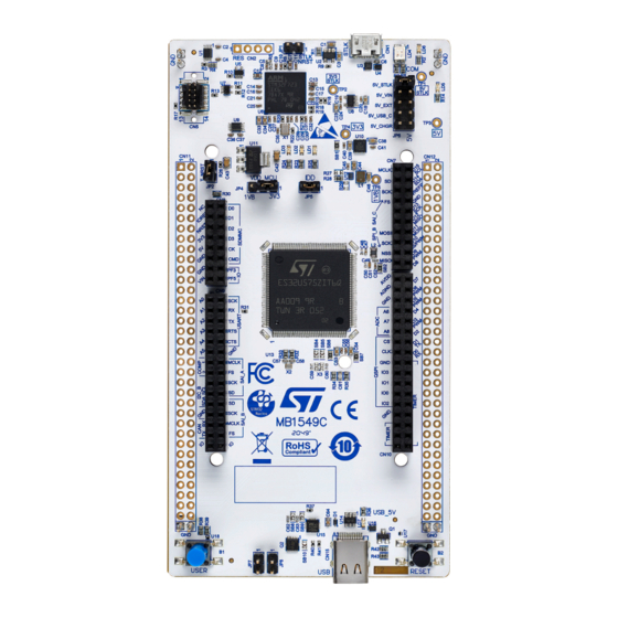
Figure 1.
STM32U5 Nucleo-144 board
Picture is not contractual.
UM2861 - Rev 2 - September 2021
www.st.com
For further information contact your local STMicroelectronics sales office.
Advertisement
Table of Contents

Related Manuals for ST STM32U5


Summary of Contents for ST STM32U5
-
Page 1: Figure 1. Stm32U5 Nucleo-144 Board
STM32 Nucleo open development platform with a wide choice of specialized shields. The STM32U5 Nucleo-144 board does not require any separate probe as it integrates the STLINK-V3E debugger/programmer. The STM32U5 Nucleo-144 board comes with the STM32 comprehensive free software libraries and examples available with the STM32CubeU5 MCU Package. -
Page 2: Features
® – ST Zio connector including ARDUINO Uno V3 – ST morpho extension pin headers for full access to all STM32 I/Os • Flexible power-supply options: ST-LINK, USB V , or external sources • On-board STLINK-V3E debugger/programmer with USB re-enumeration capability: mass storage, Virtual COM port, and debug port •... -
Page 3: Ordering Information
The meaning of the codification is explained in Table 1. Table 2. Codification explanation NUCLEO-XXYYZE-Q Description Example: NUCLEO-U575ZI-Q MCU series in STM32 Arm Cortex MCUs STM32U5 Series MCU product line in the series STM32U575/585 STM32 package pin count 144 pins STM32 Flash memory size: •... -
Page 4: Development Environment
STM32 Flash memory for easy demonstration of the device peripherals in standalone mode. The latest versions of the demonstration source code and associated documentation can be downloaded from www.st.com. UM2861 - Rev 2 page 4/49... -
Page 5: Conventions
UM2861 Conventions Conventions Table 3 provides the conventions used for the ON and OFF settings in the present document. Table 3. ON/OFF convention Convention Definition Jumper JPx ON Jumper fitted Jumper JPx OFF Jumper not fitted Jumper JPx [1-2] Jumper fitted between Pin 1 and Pin 2 Solder bridge SBx ON SBx connections closed by 0 Ω... -
Page 6: Quick Start
Develop your application using the available examples. Default board configuration By default, the STM32U5 Nucleo-144 board is configured with VDD_MCU@3V3. It is possible to set the board for VDD_MCU@1V8. Before switching to 1V8, check that the extension module and external shield connected to the NUCLEO board are 1.8 V compatible. -
Page 7: Figure 2. Default Board Configuration
UM2861 Default board configuration Figure 2. Default board configuration UM2861 - Rev 2 page 7/49... -
Page 8: Table 5. Jumper Configuration
UM2861 Default board configuration Table 5 explains the other jumper settings and configurations. Table 5. Jumper configuration Jumper Definition Setting Comment Use to reset the STLINK-V3E MCU when an external debug probe is used. STLK_RST Normal mode: use the STLINK-V3E debug probe STLINK-V3E able to reset target MCU STLINK-V3E not able to reset Target... -
Page 9: Hardware Layout And Configuration
UM2861 Hardware layout and configuration Hardware layout and configuration The STM32U5 Nucleo-144 board is designed around an STM32U5 microcontroller in an LFQFP 144-pin package. Figure 3 shows the connections between the STM32 and its peripherals (STLINK-V3E, push‑buttons, LEDs, USB ST Zio connectors, and ST morpho headers). -
Page 10: Stm32U5 Nucleo-144 Board Layout
UM2861 STM32U5 Nucleo-144 board layout STM32U5 Nucleo-144 board layout Figure 4. STM32U5 Nucleo-144 board top layout UM2861 - Rev 2 page 10/49... -
Page 11: Figure 5. Stm32U5 Nucleo-144 Board Bottom Layout
UM2861 STM32U5 Nucleo-144 board layout Figure 5. STM32U5 Nucleo-144 board bottom layout UM2861 - Rev 2 page 11/49... -
Page 12: Mechanical Drawing
UM2861 Mechanical drawing Mechanical drawing Figure 6. STM32U5 Nucleo-144 board mechanical drawing (in millimeter) UM2861 - Rev 2 page 12/49... -
Page 13: Embedded Stlink-V3E
Embedded STLINK-V3E There are two different ways to program and debug the onboard STM32 MCU: • Using the STLINK-V3E programming and debugging tool on the STM32U5 Nucleo-144 • Using an external debug tool connected to the CN5 STDC14/MIPI-10 connector ®... -
Page 14: Drivers
In case the STM32U5 Nucleo-144 board is connected to the PC before the driver is installed, a peripheral may be declared as “Unknown” in the PC device manager. In this case, the user must install or update the driver files from... -
Page 15: Using An External Debug Tool To Program And Debug The On-Board Stm32
STLINK-V3E is in RESET state and all GPIOs are in high impedance. Remove JP2 to avoid driving MCU T_NRST. Then, connect the external debug tool to the CN5 STDC14/MIPI‑10 debug connector. Figure 8. Connecting an external debug tool to program the on-board STM32U5 UM2861 - Rev 2 page 15/49... -
Page 16: Table 7. Cn5 Stdc14/Mipi-10 Debug Connector Pinout
UM2861 Embedded STLINK-V3E Figure 9 shows the CN5 STDC14/MIPI-10 connector. Figure 9. CN5 STDC14/MIPI-10 debug connector Table 7 describes the STDC14/MIPI-10 connector pinout. Table 7. CN5 STDC14/MIPI-10 debug connector pinout MIPI-10 pin STDC14 pin Function Reserved Reserved Target VDD Target SWDIO using SWD protocol or target JTMS (T_JTMS) using T_SWDIO JTAG protocol Ground... -
Page 17: Power Supply And Power Selection
This power switch also features a 500 mA current limitation, to protect the PC in case of an onboard short-circuit. The STM32U5 Nucleo-144 board with its shield can be powered from the CN1 STLINK-V3E USB connector, but only the STLINK-V3E circuit has the power before USB enumeration because the host PC only provides 100mA to the board at that time. -
Page 18: Figure 10. Jp6 [1-2]: 5V_Stlk Power Source
UM2861 Power supply and power selection • If the host is not able to provide the requested current, the enumeration fails. Therefore, the U2 power switch remains OFF and the MCU part including the extension board is not powered. As a consequence, the LD5 green LED remains OFF. -
Page 19: Figure 11. Jp6 [3-4]: 5V_Vin Power Source
VIN (5V_VIN) is the 7 to 12 V DC power from the CN8 ARDUINO the connector silkscreen, or from the CN11 ST morpho connector pin 24. In this case, the JP6 jumper must be on pin [3-4] to select the 5V_VIN power source. In that case, the DC power comes from the power supply through the ®... -
Page 20: Figure 12. Jp6 [5-6]: 5V_Ext Power Source
Power supply and power selection 5V_EXT is the DC power coming from an external 5 V DC power from the CN11 ST morpho connector pin 6. In this case, the JP6 jumper must be set on [5-6] to select the 5V_EXT power source. -
Page 21: Figure 13. Jp6 [7-8]: 5V_Usb_C Power Source
UM2861 Power supply and power selection ® 5V_USB_C is the DC power supply connected to the CN15 user USB Type-C connector. In this case, the JP6 jumper must be set on [7-8] to select the 5V_USB_C power source. 5V_USB_C configuration: The JP6 jumper must be set on [7-8] as shown in Figure Figure 13. -
Page 22: Figure 14. Jp6 [9-10]: 5V_Chgr Power Source
UM2861 Power supply and power selection 5V_CHGR is the DC power charger connected to the CN1 USB STLINK-V3E connector. In this case, the JP6 jumper must be set on [9-10] to select the 5V_CHGR power source. If an external USB charger powers the Nucleo board, then the debug through CN1 is not available. -
Page 23: Programing/Debugging When The Power Supply Is Not From Stlink-V3E (5V_Stlk)
UM2861 Power supply and power selection External 3V3 power supply input. In certain situations, it is interesting to use an external 3V3 (CN8 pin 7, CN11 pin 16, or JP5 pin 2) directly as power input, for instance in case the 3V3 is provided by an extension board. When Nucleo is powered by 3V3, the STLINK-V3E is not powered thus programming and debug features are unavailable. -
Page 24: Mcu Power Supply
Warning: 1V8 voltage is given as an example, but the power on sequence implementation is not respected when using 1V8 VDD. Refer to the application note STM32U5 Series hardware getting started (AN5373), and STM32U5xx products datasheets for power sequencing. INTERNAL VCORE SMPS power supply... -
Page 25: Vdd_Mcu Idd Measurement
The LD1 green user LED is connected to the PC7 STM32 I/O (SB21 ON and SB23 OFF, default configuration) or PA5 (SB21 OFF and SB23 ON, optional configuration corresponding to the D13 ST Zio connector). A transistor is used to drive the LED whatever the MCU 1V8 or 3V3 voltage range is. -
Page 26: Push-Buttons
UM2861 Push-buttons Push-buttons Two buttons are available on the Nucleo board. B1 USER button The blue button for user and wake‑up functions is connected to PC13 to support the default TAMPER function or to PA0 to support the optional wake‑up function of the STM32 Microcontroller. When the button is pressed the logic state is HIGH, otherwise, the logic state is LOW. -
Page 27: Osc Clock Supply
The reset signal of the Nucleo board is active LOW and the reset sources include: • The RESET button B2 • The embedded STLINK-V3E ® • The CN8 ARDUINO -included Zio connector pin 5 • The CN11 ST morpho connector pin 14 UM2861 - Rev 2 page 27/49... -
Page 28: Virtual Com Port (Vcp)
Uno V3, and ST morpho connectors is enabled on LPUART1, not to interfere with the VCP interface. PG7 and PG8 are also connected to the CN12 ST morpho connector pin 66 (SB72) and 67 (SB73). The two ® solder bridges can be removed in case of conflict between ARDUINO Uno V3 and ST morpho for PG7 or PG8. -
Page 29: Usb Type-C ® Fs
No other muxing PA11 SB40 PA11 can be used as an I/O on the ST morpho connector. USB function can be used, but performances are low due to the track length to the Zio connector causing impedance mismatch. PA12 used as USB_FS_P diff pair interface... -
Page 30: Usb Type-C Connector
IO UCPD_FLT connected to USB Type-C port protection and used as over‑voltage fault reporting to MCU SB45 PB14 not used for UCPD_FLT can be used on the ST morpho connector PB14 UCPD_DBCC2 connected to GND (only for internal UCPD debug... -
Page 31: Table 14. Cn15 Usb Type-C ® Connector Pinout
UM2861 USB Type-C® FS ® Table 14 describes the pinout of the USB Type-C connector CN15. ® Table 14. CN15 USB Type-C connector pinout STM32 pin Signal name Pin name Pin name Signal name STM32 pin TX1+ RX1+ TX1- RX1- VBUS_C/ VBUS_C/ VBUS... -
Page 32: Extension Connectors
Most of the STM32 microcontroller I/Os are 5 V‑tolerant, but few of them are only 3V3‑compatible, while ® ARDUINO Uno V3 is 5 V‑compatible. Refer to the STM32U5 Series data brief and STM32U5xx product datasheets for their I/O structure. ®... -
Page 33: Table 15. Cn7 Arduino ® -Included Zio Connector Pinout
UM2861 Zio connectors supporting ARDUINO® Uno V3 ® Table 15. CN7 ARDUINO -included Zio connector pinout STM32 STM32 Signal name Pin name Pin name Signal name function function SAI2_A SAI_C_MCLK I2C_A_SCL I2C1 SAI2_A PD11 SAI_C_SD I2C_A_SDA I2C1 SAI2_A PB13 SAI_C_SCK VREFP SAI2_A PD12... -
Page 34: Table 17. Cn9 Arduino ® -Included Zio Connector Pinout
UM2861 Zio connectors supporting ARDUINO® Uno V3 ® Table 17. CN9 ARDUINO -included Zio connector pinout STM32 STM32 Signal name Pin name Pin name Signal name function function USART_B_SCL ADC1_IN8 PA3 USART2 ADC1_IN7 PA2 USART_B_RX USART2 ADC1_IN4 PC3 USART_B_TX USART2 ADC1_IN1 USART_B_RTS USART2... - Page 35 UM2861 Zio connectors supporting ARDUINO® Uno V3 STM32 STM32 Signal name Pin name Pin name Signal name function function TIM1_CH1 PA8 TIM_D_PWM1 TIM_C_PWM2 PB10 TIM2_CH3 TIM4_ETR PE0 TIM_B_ETR TIM_C_PWM3 PB11 TIM2_CH4 1. The default configuration for the D0/D1 signal is LPUART1 on PG7 and PG8, USART1 on PA9 and PA10 is connected by default on STLINK-V3E.
-
Page 36: Cn11 And Cn12 St Morpho Headers
STM32 Nucleo-144 board to an extension board or a prototype/wrapping board placed on top of the STM32 Nucleo-144 board. All signals and power pins of the STM32 are available on the ST morpho connector. An oscilloscope, a logic analyzer, or a voltmeter can also probe this connector. -
Page 37: Table 19. St Morpho Connector Pin Assignment
UM2861 CN11 and CN12 ST morpho headers Table 19. ST morpho connector pin assignment CN11 odd pins CN11 even pins CN12 odd pins CN12 even pins Pin number Pin name Pin number Pin name Pin number Pin name Pin number Pin name... -
Page 38: Solder Bridge Configuration For The Expansion Connector
UM2861 Solder bridge configuration for the expansion connector Solder bridge configuration for the expansion connector Table 20 details the solder bridges of the STM32U5 Nucleo-144 board for the expansion connector. Table 20. Solder bridge configuration Definition Bridge Setting Comment IOREF not connected to 1V8 power supply... - Page 39 UM2861 Solder bridge configuration for the expansion connector Definition Bridge Setting Comment SB61 PB10 used as QSPI_CLK PB10 PB10 not used as TIMER for motor Control SB62 PB10 used as TIMER for motor Control PA0 not used as TIMER for motor control, reserved for User TIMER_C_PWM1 / button User-Button...
-
Page 40: Nucleo-U575Zi-Q Board Information
Evaluation tools marked as “ES” or “E” are not yet qualified and therefore not ready to be used as reference design or in production. Any consequences deriving from such usage will not be at ST charge. In no event, ST will be liable for any customer usage of these engineering sample tools as reference designs or in production. -
Page 41: Board Revision History
UM2861 Board revision history Board revision history 8.3.1 Board MB1549‑C02 The revision C02 of the MB1549 board is the first official version. Board limitation SWDIO: Because of the level shifter to support 1V8 MCU debug, it is recommended to set the SWDIO frequency to 8 MHz. -
Page 42: Federal Communications Commission (Fcc) And Innovation, Science And Economic
UM2861 Federal Communications Commission (FCC) and Innovation, Science and Economic Development Canada (ISED) Compliance Statements Federal Communications Commission (FCC) and Innovation, Science and Economic Development Canada (ISED) Compliance Statements FCC Compliance Statement Part 15.19 This device complies with Part 15 of the FCC Rules. Operation is subject to the following two conditions: (1) this device may not cause harmful interference, and (2) this device must accept any interference received, including interference that may cause undesired operation. -
Page 43: Ce Conformity
UM2861 CE conformity CE conformity 10.1 Warning EN 55032 / CISPR32 (2012) Class B product Warning: this device is compliant with Class B of EN55032 / CISPR32. In a residential environment, this equipment may cause radio interference. Avertissement : cet équipement est conforme à la Classe B de la EN55032 / CISPR 32. Dans un environnement résidentiel, cet équipement peut créer des interférences radio. -
Page 44: Revision History
UM2861 Revision history Table 21. Document revision history Date Version Changes 24-Jun-2021 Initial release. Added Product limitation Product identification NUU575ZIQ$AT1 13-Sep-2021 Product identification NUU575ZIQ$AT2 solving this limitation. UM2861 - Rev 2 page 44/49... -
Page 45: Table Of Contents
STM32U5 Nucleo-144 board layout ........ - Page 46 CN11 and CN12 ST morpho headers ........
-
Page 47: List Of Tables
ST morpho connector pin assignment........ -
Page 48: List Of Figures
STM32U5 Nucleo-144 board mechanical drawing (in millimeter) ....... . . - Page 49 ST’s terms and conditions of sale in place at the time of order acknowledgement. Purchasers are solely responsible for the choice, selection, and use of ST products and ST assumes no liability for application assistance or the design of Purchasers’...
Need help?
Do you have a question about the STM32U5 and is the answer not in the manual?
Questions and answers