Table of Contents
Advertisement
Quick Links
UM3062
User manual
STM32U5 Nucleo-64 board (MB1841)
Introduction
The Nucleo-64 board based on the MB1841 reference board (NUCLEO-U545RE-Q) provides an affordable and flexible way
for users to try out new concepts and build prototypes by choosing from the various combinations of performance and power
consumption features, provided by the STM32U5 series microcontroller.
®
The ARDUINO
Uno V3 connectivity and the ST morpho headers provide easy expansion of the functionality of the STM32
Nucleo open development platform with a wide choice of specialized shields.
The STM32 Nucleo-64 board does not require any separate probe as it integrates the STLINK-V3EC debugger/programmer.
The STM32 Nucleo-64 board comes with the STM32 comprehensive free software libraries and examples available with the
STM32CubeU5
MCU Package.
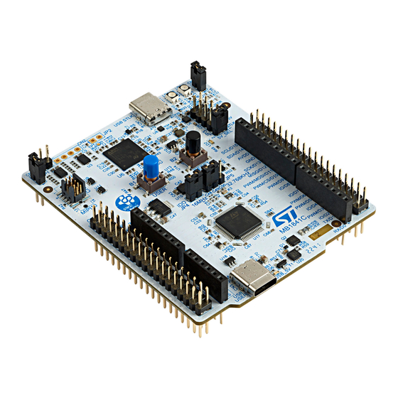
Figure 1.
Nucleo-64 board (top view)
Picture is not contractual.
UM3062 - Rev 1 - April 2023
www.st.com
For further information contact your local STMicroelectronics sales office.
Advertisement
Table of Contents

Related Manuals for ST STM32U5 Nucleo-64


Summary of Contents for ST STM32U5 Nucleo-64
-
Page 1: Figure 1. Nucleo-64 Board (Top View)
® The ARDUINO Uno V3 connectivity and the ST morpho headers provide easy expansion of the functionality of the STM32 Nucleo open development platform with a wide choice of specialized shields. The STM32 Nucleo-64 board does not require any separate probe as it integrates the STLINK-V3EC debugger/programmer. -
Page 2: Features
® – ARDUINO Uno V3 – ST morpho extension pin headers for full access to all STM32 I/Os • Flexible power-supply options: ST-LINK USB V , user USB connector, or external sources • On-board STLINK-V3EC debugger/programmer with USB re-enumeration capability: mass storage, Virtual COM port, and debug port •... -
Page 3: Ordering Information
UM3062 Ordering information Ordering information To order the Nucleo-64, refer to Table 1. Additional information is available from the datasheet and reference manual of the target STM32. Table 1. Ordering information Order code Board reference Target STM32 Differentiating feature Microcontroller featuring NUCLEO-U545RE-Q MB1841 STM32U545RET6Q... -
Page 4: Development Environment
UM3062 Development environment Development environment System requirements ® ® ® • Multi‑OS support: Windows 10, Linux 64-bit, or macOS ® ® • USB Type-A or USB Type-C to USB Type-C cable Note: ® macOS is a trademark of Apple Inc., registered in the U.S. and other countries and regions. ®... -
Page 5: Conventions
UM3062 Conventions Conventions Table 3 provides the conventions used for the ON and OFF settings in the present document. Table 3. ON/OFF convention Convention Definition Jumper JPx ON Jumper fitted Jumper JPx OFF Jumper not fitted Jumper JPx [1-2] Jumper fitted between Pin 1 and Pin 2 Solder bridge SBx ON SBx connections closed by 0 Ω... -
Page 6: Quick Start
STM32U5 series microcontroller in an LQFP 64‑pin package. Before installing and using the product, accept the Evaluation Product License Agreement from the www.st.com/epla webpage. For more information on the STM32 Nucleo-64 board and for the software example, visit the www.st.com/stm32nucleo... -
Page 7: Figure 2. Default Board Configuration
UM3062 Default board configuration Figure 2. Default board configuration JP3 [1-2 ] JP5 [1-2 ] JP4 [1-2 ] STM32 microcontroller UM3062 - Rev 1 page 7/45... -
Page 8: Table 5. Jumper Configuration
[3-4] from CN6 or CN7 5V source from external 5V (E5V) from [5-6] CN6 or CN7 5V power selection 5V source from ST-LINK in USB charger [7-8] mode without USB negociation (CN1) ® 5V source from user USB Type-C [9-10] (CN3) No 5V power source. -
Page 9: Hardware Layout And Configuration
The STM32 Nucleo-64 board is designed around an STM32U5 microcontroller in an LQFP 64‑pin package. Figure 3 shows the connections between the STM32 and its peripherals (STLINK-V3EC, push‑buttons, LEDs, ® USB, ARDUINO connectors, and ST morpho headers). Figure 4 Figure 5 show the location of these features on the STM32 Nucleo-64 board. -
Page 10: Nucleo-64 Board Layout
(LD4) STLK COM LED (LD1) 5V LED (LD3) MIPI10 (CN14) 5V jumper selection (JP3) User button Reset button (B1) (B1) ST morpho connector ST morpho connector (CN10) (CN7) VDD selection 3V3/1V8 IDD jumper (JP5) (JP4) ® ARDUINO D[15-8] ® ARDUINO... -
Page 11: Figure 5. Nucleo-64 Board Bottom Layout
UM3062 Nucleo-64 board layout Figure 5. Nucleo-64 board bottom layout SN sticker CPN sticker UM3062 - Rev 1 page 11/45... -
Page 12: Mechanical Drawing
UM3062 Mechanical drawing Mechanical drawing Figure 6. Nucleo-64 board mechanical drawing (in millimeters) UM3062 - Rev 1 page 12/45... -
Page 13: Embedded Stlink-V3Ec
The chapter below gives some information about the implementation of the STLINK-V3EC on this Nucleo-64 board. For details information about ST-LINK capabilities, LED management, driver, and firmware for this STLINK-V3EC, refer to the technical note Overview of ST-LINK derivatives (TN1235). -
Page 14: Drivers
The driver installation is not mandatory since Windows 10 but allocates an ST-specific name to the ST-LINK COM port in the system device manager. For details information on the ST-LINK USB driver, refer to the technical note Overview of ST-LINK derivatives (TN1235). 6.3.3 STLINK-V3EC firmware upgrade The STLINK-V3EC embeds a firmware upgrade (stsw_link007) mechanism through the USB port. -
Page 15: Using An External Debug Tool To Program And Debug The On-Board Stm32
UM3062 Embedded STLINK-V3EC 6.3.4 Using an external debug tool to program and debug the on-board STM32 To support an external debug tool, set the jumper (JP1) to isolate the output I/O from STLINK-V3EC. Then connect the external debug tool through the STDC14/MIPI10 debug connector (CN4). When using the external debug connector (CN4), it is possible to use the STLINK-V3EC USB connector (CN1) to supply the Nucleo-64 board or select another power supply source as described in Section 6.4 Power supply and... -
Page 16: Table 6. Stdc14/Mipi10 Debug Connector (Cn4) Pinout
UM3062 Embedded STLINK-V3EC Figure 8 shows the STDC14/MIPI10 connector (CN4). Figure 8. STDC14/MIPI10 debug connector (CN4) STDC14/MIPI10 (CN4) Table 6. STDC14/MIPI10 debug connector (CN4) pinout describes the STDC14/MIPI10 connector (CN4) pinout. Table 6. STDC14/MIPI10 debug connector (CN4) pinout MIPI10 pin STDC14 pin Function Reserved... -
Page 17: Power Supply And Power Selection
(CN1) ® • VIN: 7 to 12V from ARDUINO (CN6) or ST morpho connector (CN7), with 5 V adaptation from LDO (U16) • E5V: External 5 V power from ST morpho connector (CN7) • CHGR: 5 V from STLINK-V3EC USB (CN1) without USB enumeration ®... -
Page 18: Figure 9. 5V Jumper Selection Jp3[1-2]: Stlk Power Source
UM3062 Power supply and power selection STLK is a 5 V DC power with limitations from the STLINK-V3EC USB connector (CN1). In this case, the 5V jumper selection (JP3) must be on pin [1-2] to select the STLK power source on the JP3 connector. This is the default setting. -
Page 19: Figure 10. 5V Jumper Selection Jp3[3-4]: Vin_5V Power Source
VIN (VIN_5V) is the 7 to 12 V DC power source from the ARDUINO connector (CN6) pin 8 (VIN), or from the ST morpho connector (CN7) pin 24. The 5V jumper selection (JP3) must be on pin [3‑4] to select VIN_5V ®... -
Page 20: Figure 11. 5V Jumper Selection Jp3[5-6]: E5V Power Source
Power supply and power selection E5V is the DC power coming from an external 5 V dc power source from the ST morpho connector (CN7) pin 6. The 5V jumper selection (JP3) must be on pin [5-6] to select the E5V power source on the JP3 connector and must be connected as shown in Figure 11. -
Page 21: Figure 12. 5V Jumper Selection Jp3[7-8]: Chgr Power Source
UM3062 Power supply and power selection CHGR is when a DC power charger is connected to the USB STLINK-V3EC (CN1). To select the CHGR power source, the 5V jumper selection (JP3) must be on pins [7-8]. If an external USB charger powers the Nucleo-64 board, then the debugging feature through (CN1) is not available. -
Page 22: Figure 13. 5V Jumper Selection Jp3[9-10]: Usb User Power Source
UM3062 Power supply and power selection ® USB_USER is the DC power source coming from the 5 V of the USB Type-C connector (CN3). The 5V jumper selection (JP3) must be on pins [9-10] and must be connected as shown in Figure Figure 13. -
Page 23: Programing/Debugging When The Power Supply Is Not From Stlink-V3Ec (Stlk)
In case the current consumption of the Nucleo-64 and the expansion boards exceeds the allowed current on the ST-LINK USB connector, the external power VIN, E5V, or USB-USER can be used. In such a case, it is still possible to use the embedded ST-LINK for VCP, programming and debugging. -
Page 24: Mcu Power Supply
VDD, such as the level shifter power supply pins for STLINK-V3EC, the user button, ® ARDUINO shield on the IOREF pin, and power supply pins on the ST morpho connector. 6.4.5 MCU power supply The default configuration of the MCU power pins is described in Table Table 8. -
Page 25: Leds
The tricolor (green, orange, and red) LEDs provide information about STLINK-V3EC communication status (LD1) and power status (LD4). For detailed information about these LEDs, refer to the technical note Overview of ST-LINK derivatives (TN1235). User green LED (LD2) The user green LED (LD2) is connected to the STM32 I/O PA5 (SB10 ON, default configuration) also used for ®... -
Page 26: Osc Clock Sources
• SB1 and SB2 ON • SB18 and SB22 OFF External oscillator connected to PC14 input From the external oscillator through pin 25 of the ST morpho connector (CN7). The following configuration is needed: • SB1 and SB2 OFF •... -
Page 27: Reset Sources
Uno V3 D0/D1 1. The default configuration is in bold. By default: • The serial communication between the target MCU and ST-LINK MCU is enabled on USART1 because this interface supports the Bootloader mode. ® • The serial communication between the target MCU and ARDUINO Uno V3 or ST morpho connector is enabled on LPUART1, not to interfere with the VCP interface. -
Page 28: Bootloader
6.10 Bootloader The bootloader is located in the system memory, programmed by ST during production. It is used to reprogram the flash memory via USART, I C, SPI, CAN FD, or USB FS in device mode through the device firmware upgrade (DFU). -
Page 29: Usb Type-C ® Fs
Configuration channel: UCPD_CCx and Dead battery UCPD_DBn: As the STM32 Nucleo-64 supports only Sink current mode with 5 V and 500 mA (2.5 W), these signals are directly connected to the ground through the ST USB port protection TCPP01-M12. •... -
Page 30: Usb Type-C Connector
UM3062 USB Type-C® FS Table 11 describes the hardware configuration for the UCPD feature. Table 11. Hardware configuration for the UCPD feature Solder bridge Setting Configuration PC2 used as VBUS_SENSE SB31 PC2 NOT used for UCPD. It can be used on the expansion connector. 1. -
Page 31: Extension Connectors
Six extension connectors are implemented on the board: ® • ARDUINO Uno V3 connectors (CN5, CN6, CN8, and CN9) • ST morpho connectors (CN7 and CN10) ® ARDUINO Uno V3 ® The CN5, CN6, CN8, and CN9 connectors are female connectors supporting the ARDUINO Uno V3 standard. -
Page 32: Table 13. Arduino ® Power Connector (Cn6) Pinout
UM3062 ARDUINO® Uno V3 ® Table 13. ARDUINO power connector (CN6) pinout Pin name Signal name STM32 pin MCU function RESERVED IOREF IOREF IO REF NRST NRST NRST RESET 3V3 input/output 5V output VIN (7-12V) ® Table 14. ARDUINO ADC connector (CN8) pinout Pin name Signal name STM32 pin... -
Page 33: Table 16. Arduino ® D[15-8] Connector (Cn5) Pinout
UM3062 ARDUINO® Uno V3 ® Table 16. ARDUINO D[15-8] connector (CN5) pinout Pin name Signal name STM32 pin MCU function I2C_SCL I2C1_SCL / I2C4_SCL I2C_SDA I2C1_SDA / I2C4_SDA VREFP SPI_SCK SPI1_SCK SPI_MISO SPI1_MISO SPI_MOSI / PWM SPI1_MOSI / TIM3_CH2 SPI_NSS / PWM SPI_NSS / TIM3_CH4 TIM3_CH1 1. -
Page 34: St Morpho Headers (Cn7 And Cn10)
ST morpho headers (CN7 and CN10) The ST morpho connector consists of CN7 and CN10 2.54‑pitch male pin header. They can be used to connect the STM32 Nucleo-64 board to an extension or a prototype/wrapping board placed on top of it. All signals and power pins of the STM32 are available on the ST morpho connector. -
Page 35: Table 17. St Morpho Connector Pin Assignment
UM3062 ST morpho headers (CN7 and CN10) Table 17. ST morpho connector pin assignment CN7 odd pins CN7 even pins CN10 odd pins CN10 even pins Pin number Pin name Pin number Pin name Pin number Pin name Pin number... -
Page 36: Solder Bridge Configuration For The Expansion Connector
UM3062 Solder bridge configuration for the expansion connector Solder bridge configuration for the expansion connector Table 18 details the solder bridges of the STM32 Nucleo-64 board for the expansion connector. Table 18. Solder bridge configuration Definition Bridge Setting (1)(2) Comment IOREF is not connected to the VDD power supply. -
Page 37: Nucleo-U545Re-Q Board Information
B01. The second line shows the board serial number used for traceability. Parts marked as “ES” or “E” are not yet qualified and therefore not approved for use in production. ST is not responsible for any consequences resulting from such use. In no event will ST be liable for the customer using any of these engineering samples in production. -
Page 38: Nucleo-U545Re-Q Product History
UM3062 NUCLEO-U545RE-Q product history NUCLEO-U545RE-Q product history Table 19. Product history Order Product Product details Product change description Product limitations code identification MCU: • STM32U545RET6Q silicon revision A MCU errata sheet: NUU545REQ$MR1 Initial revision No limitation • STM32U535xx and STM32U545xx device errata (ES0587) Board: •... -
Page 39: Federal Communications Commission (Fcc) And Ised Canada Compliance
UM3062 Federal Communications Commission (FCC) and ISED Canada Compliance Statements Federal Communications Commission (FCC) and ISED Canada Compliance Statements FCC Compliance Statement Part 15.19 This device complies with Part 15 of the FCC Rules. Operation is subject to the following two conditions: (1) this device may not cause harmful interference, and (2) this device must accept any interference received, including interference that may cause undesired operation. -
Page 40: Revision History
UM3062 Revision history Table 21. Document revision history Date Revision Changes 3-Apr-2023 Initial release. UM3062 - Rev 1 page 40/45... -
Page 41: Table Of Contents
UM3062 Contents Contents Features................2 Ordering information . - Page 42 ST morpho headers (CN7 and CN10) ........
-
Page 43: List Of Tables
ST morpho connector pin assignment........ -
Page 44: List Of Figures
ST morpho connector ........ - Page 45 ST’s terms and conditions of sale in place at the time of order acknowledgment. Purchasers are solely responsible for the choice, selection, and use of ST products and ST assumes no liability for application assistance or the design of purchasers’...
Need help?
Do you have a question about the STM32U5 Nucleo-64 and is the answer not in the manual?
Questions and answers