Table of Contents
Advertisement
UM3223
User manual
Discovery kit with STM32U5G9ZJ MCU
Introduction
The
STM32U5G9J-DK2
Discovery kit is a complete demonstration and development platform for the
STM32U5G9ZJT6Q
®
®
‑M33 core with Arm
®
®
microcontroller, featuring an Arm
Cortex
TrustZone
.
Leveraging the innovative ultra-low power-oriented features, 3 Mbytes of embedded SRAM, 4 Mbytes of embedded flash
memory, and rich graphics features, the STM32U5G9J-DK2 Discovery kit enables users to prototype applications with
state‑of‑the‑art energy efficiency, as well as providing stunning and optimized graphics rendering with the support of a 2.5D
™
Neo-Chrom accelerator, Chrom-ART Accelerator, and Chrom-GRC
MMU.
The STM32U5G9J-DK2 Discovery kit integrates a full range of hardware features that help the user evaluate all the peripherals,
such as a 5" RGB 800x480 pixels TFT colored LCD module with a 24‑bit RGB interface and capacitive touch panel, high-speed
®
®
USB Type-C
, Octo‑SPI flash memory device, ARDUINO
, and STLINK-V3EC (USART console).
The STM32U5G9J-DK2 Discovery kit integrates an STLINK-V3EC embedded in-circuit debugger and programmer for the
STM32 microcontroller with a USB Virtual COM port bridge and comes with the
STM32CubeU5
MCU Package, which provides
an STM32 comprehensive software HAL library as well as various software examples.
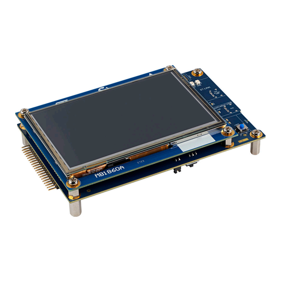
Figure 1.
STM32U5G9J-DK2
Figure 2.
STM32U5G9J-DK2
Figure 3.
STM32U5G9J-DK2
with LCD (top view)
without LCD (top view)
(bottom view)
Pictures are not contractual.
UM3223 - Rev 1 - January 2024
www.st.com
For further information contact your local STMicroelectronics sales office.
Advertisement
Table of Contents

Related Manuals for ST STM32U5G9J-DK2


Summary of Contents for ST STM32U5G9J-DK2
-
Page 1: Figure 1. Stm32U5G9J-Dk2 With Lcd (Top View)
MMU. The STM32U5G9J-DK2 Discovery kit integrates a full range of hardware features that help the user evaluate all the peripherals, such as a 5" RGB 800x480 pixels TFT colored LCD module with a 24‑bit RGB interface and capacitive touch panel, high-speed ®... -
Page 2: Features
Low-power system designed for VDD at 3.3 V only • 1-Gbit Octo‑SPI flash memory • Two user LEDs • User and reset push-buttons • Board connectors: ® – ST-LINK USB Type-C ® – User USB Type-C ® ® – Cortex MIPI10 connector (SWD/JTAG/trace) ™ –... -
Page 3: Ordering Information
The meaning of the codification is explained in Table Table 2. Codification explanation STM32XXYYZ-DKT Description Example: STM32U5G9J-DK2 MCU series in STM32 32-bit Arm Cortex MCUs STM32U5 series MCU product line in the series STM32U5F9/5G9 product line STM32 flash memory size: 4 Mbytes •... -
Page 4: Development Environment
STM32 flash memory for easy demonstration of the device peripherals in standalone mode. The latest versions of the demonstration source code and associated documentation can be downloaded from www.st.com. UM3223 - Rev 1 page 4/37... -
Page 5: Conventions
UM3223 Conventions Conventions Table 3 provides the conventions used for the ON and OFF settings in the present document. Table 3. ON/OFF convention Convention Definition Jumper JPx ON Jumper fitted Jumper JPx OFF Jumper not fitted Jumper JPx [1-2] Jumper fitted between Pin 1 and Pin 2 Solder bridge SBx ON SBx connections closed by 0 Ω... -
Page 6: Quick Start
(STLK) and JP4 (VDD_MCU current measurement) is ON powering the microcontroller. Refer to Table ® 3. Connect the STM32U5G9J-DK2 Discovery board to a PC with a USB cable (USB Type-A or USB Type-C ® USB Type-C ) through the STLINK-V3EC USB connector (CN8) to power the board. -
Page 7: Hardware Layout And Configuration
Figure 4 illustrates the connection between the STM32U5G9ZJT6Q microcontroller and the peripherals. Figure 5 Figure 6 show the locations of these features on the STM32U5G9J-DK2 Discovery board. Figure 4. STM32U5G9J-DK2 hardware block diagram STM32U5G9ZJT6Q External debug ®... -
Page 8: Main Board Layout
Figure 6. Main board layout (bottom view) RGB LCD connector Tag-Connect™ (CN3) footprint (CN10) ST-LINK power LED (LD6) ST-LINK COM LED (LD7) 5V power LED (LD1) 5V USB power (LD5) User red LED (LD2) User green LED (LD3) User button (B2) -
Page 9: Mechanical Drawing
UM3223 Hardware layout and configuration Mechanical drawing Figure 7. Main board mechanical drawing (in millimeters) UM3223 - Rev 1 page 9/37... -
Page 10: Embedded Stlink-V3Ec
Power status LED (LD6), which gives information about STLINK-V3EC target power ® • USB-C overvoltage protection (U16) with current limitation For detailed information about these LEDs, refer to the technical note Overview of ST-LINK derivatives (TN1235). UM3223 - Rev 1 page 10/37... -
Page 11: Drivers
Since Windows 10, driver installation is not mandatory. Anyway, it is highly recommended as it allocates an ST‑specific name to the ST-LINK COM port in the system device manager. For detailed information on the ST-LINK USB drivers, refer to the technical note Overview of ST-LINK derivatives (TN1235). -
Page 12: Table 6. Tag-Connect ™ Footprint (Cn10) Pinout For Tc2050-Idc-Nl Cable
UM3223 Hardware layout and configuration ™ Table 6. Tag‑Connect footprint (CN10) pinout for TC2050-IDC-NL cable CN10 pin Signal Function Target VDD (indication to the probe) Target SWDIO using SWD protocol or target JTMS (T_JTMS) using JTAG JTMS_SWDIO protocol Ground Target SWCLK using SWD protocol or target JTCK (T_JTCK) using JTAG JTCK_SWCLK protocol Ground... -
Page 13: Power Supply
UM3223 Hardware layout and configuration Power supply Figure 9. STM32U5G9J-DK2 power diagram ST-LINK Power selection ® USB-C Overvoltage VBUS_STLK 5V_STLK protection connector DC/DC discrete 3V3_STLK components VBUS_STLK LDO or 5V_EXT DC/DC 5V_USB Octo-SPI LEDs ® ARDUINO VEXT 5V_VEXT connector Backlight ®... -
Page 14: Supplying The Board With The Stlink-V3Ec Usb Connector (Cn8)
Tag‑Connect footprint (CN10) pinout for TC2050-IDC-NL cable Source Function [1-2] STLK 5 V is supplied from the ST-LINK USB connector (CN8) ® [3-4] 5 V is supplied from the ARDUINO connector (CN5). [5-6] 5 V is supplied from the user USB connector (CN2). -
Page 15: Supplying The Board With The Application Usb Connector (Cn2)
UM3223 Hardware layout and configuration 6.5.3 ® Supplying the board with an external power supply from the ARDUINO connector (CN5) ® In this mode, the board is powered (7 to 12 V DC) through the VIN pin of the ARDUINO compatible connector (CN5). -
Page 16: Measurement Of Microcontroller Current Consumption
UM3223 Hardware layout and configuration 6.5.5 Measurement of microcontroller current consumption The power consumption measurement of the STM32U5G9ZJT6Q MCU is possible by replacing the JP4 jumper labeled IDD with an ammeter. Figure 14. Current consumption measurement jumper (JP4) IDD MCU (JP4) Clocks 6.6.1... -
Page 17: Boot Modes
UM3223 Hardware layout and configuration Boot modes The SW1 switch selects the Boot mode thanks to the PH3/BOOT0 pin of the MCU and SWBOOT0 option byte: • Position 0 [2-1]: BOOT0 is pulled down to the ground. The code is executed from the internal flash memory (default configuration as shown in Figure •... -
Page 18: Board Functions
5, and Figure 6 STM32U5G9J-DK top and bottom layout views. ® The STM32U5G9J-DK2 board provides a USB Type-C connector (CN2) that can support a custom USB application (Sink mode only). VBUS (5 V) and CC lines have overvoltage protection The green LED (LD5) lights up when powered by a USB Host. -
Page 19: Octo-Spi Flash Memory
Virtual COM port A Virtual COM port is available on the STLINK-V3EC USB connector (CN8). The communication between the target and ST-LINK MCUs is enabled on the USART1 (PA9/PA10). UM3223 - Rev 1 page 19/37... -
Page 20: Buttons And Leds
UM3223 Board functions Buttons and LEDs Two buttons are available on STM32U5G9J-DK2. • Side reset button: – B1 is connected to the global reset signal (NRST of STM32U5G9ZJT6Q MCU). • Blue user button: – B2 is connected to PC13-WKUP2. –... -
Page 21: Display
Board functions Display The STM32U5G9J-DK2 Discovery kit embeds a 5-inch 800x480 TFT LCD MB1860 board, which is connected to the RGB interface of the STM32U5G9ZJT6Q MCU through a 50-pin connector (CN3). The MB1860 board uses the RK050HR18-CTG TFT LCD from Rocktech including a backlight and a capacitive touch panel. -
Page 22: Arduino ® Interface
STM32 microcontroller I/Os are 3.3 V compatible instead of 5 V for ARDUINO Uno. ® As explained in Section 6.5.3, the STM32U5G9J-DK2 board can be powered from the ARDUINO connector (CN5 VIN pin 8) with a power supply in the 7 to 12 V voltage range. ® Figure 17. -
Page 23: Table 11. Arduino ® Uno V3 Compatible Connectors
® Table 11. ARDUINO Uno V3 compatible connectors Left connectors Right connectors Connector Pin number Pin name MCU pin Function Function MCU pin Pin name Pin number Connector I2C1_SCL PG14 I2C1_SDA PG13 AVDD AVDD Ground Reserved SPI1_SCK IOREF 3V3 ref SPI1_MISO Digital RESET... -
Page 24: Gpio Extension Connector
UM3223 GPIO extension connector Spare GPIOs of the STM32U5G9ZJT6Q MCU (in DK application) are connected on a general purpose 2.54 mm pitch SAMTEC TSW-120-07-G-D extension connector (CN1). Figure 18. General extension connector (CN1) Spare GPIO connector (CN1) Table 12. General extension connector (CN1) pinout Pin number Signal Signal... -
Page 25: Stm32U5G9Zjt6Q Mcu I/O Assignment
UM3223 STM32U5G9ZJT6Q MCU I/O assignment STM32U5G9ZJT6Q MCU I/O assignment Table 13. STM32U5G9ZJT6Q I/O assignment STM32U5G9ZJT6Q signal Signal assignment Secondary function Usage TIM5_CH1 ® PWM-D6 ARDUINO GPIO interrupt USB Detect ® USART2_TX TX-D1 ARDUINO ® USART2_RX RX-D0 ARDUINO GPIO interrupt USB Fault ®... - Page 26 UM3223 STM32U5G9ZJT6Q MCU I/O assignment STM32U5G9ZJT6Q signal Signal assignment Secondary function Usage PC10 Spare GPIOs PC11 Spare GPIOs PC12 Spare GPIOs PC13 WKUP2 User interface User button LCD_B4 Display Blue 4 LCD_B5 Display Blue 5 User interface Red LED LCD_CLK Display Pixel clock User interface...
- Page 27 UM3223 STM32U5G9ZJT6Q MCU I/O assignment STM32U5G9ZJT6Q signal Signal assignment Secondary function Usage ® ADC4_IN7 ARDUINO ® ADC4_IN8 ARDUINO Spare GPIOs PG10 Spare GPIOs PG12 Spare GPIOs ® PG13 I2C1_SDA SDA-D14 ARDUINO ® PG14 I2C1_SCL SCL-D15 ARDUINO PG15 Spare GPIOs PH9-HSPI1_NCS Flash memory Chip select PH10...
-
Page 28: Stm32U5G9J-Dk2 Product Information
B01. The second line shows the board serial number used for traceability. Parts marked as “ES” or “E” are not yet qualified and therefore not approved for use in production. ST is not responsible for any consequences resulting from such use. In no event will ST be liable for the customer using any of these engineering samples in production. -
Page 29: Stm32U5G9J-Dk Product History
UM3223 STM32U5G9J-DK2 product information STM32U5G9J-DK product history Table 14. Product history Order Product identification Product details Product change description Product limitations code MCU: • STM32U5G9ZJT6Q silicon revision "Z" MCU errata sheet: • STM32U5Fxxx and STM32U5Gxxx device errata DK32U5G9J2$AR1 Initial revision... -
Page 30: Federal Communications Commission (Fcc) And Ised Canada Compliance
UM3223 Federal Communications Commission (FCC) and ISED Canada Compliance Statements Federal Communications Commission (FCC) and ISED Canada Compliance Statements 10.1 FCC Compliance Statement Contains FCC ID: P53-EMW3080. Part 15.19 This device complies with Part 15 of the FCC Rules. Operation is subject to the following two conditions: (1) this device may not cause harmful interference, and (2) this device must accept any interference received, including interference that may cause undesired operation. - Page 31 UM3223 Federal Communications Commission (FCC) and ISED Canada Compliance Statements Déclaration de conformité Avis: Le présent appareil est conforme aux CNR d'ISDE Canada applicables aux appareils radio exempts de licence. L'exploitation est autorisée aux deux conditions suivantes : (1) l'appareil ne doit pas produire de brouillage, et (2) l'utilisateur de l'appareil doit accepter tout brouillage radioélectrique subi, même si le brouillage est susceptible d'en compromettre le fonctionnement.
-
Page 32: Revision History
UM3223 Revision history Table 16. Document revision history Date Revision Changes 12-Jan-2024 Initial release. UM3223 - Rev 1 page 32/37... -
Page 33: Table Of Contents
UM3223 Contents Contents Features................2 Ordering information . - Page 34 STM32U5G9J-DK2 product information ........
-
Page 35: List Of Tables
UM3223 List of tables List of tables Table 1. List of available products............. . . 3 Table 2. -
Page 36: List Of Figures
STM32U5G9J-DK2 hardware block diagram ........ - Page 37 ST’s terms and conditions of sale in place at the time of order acknowledgment. Purchasers are solely responsible for the choice, selection, and use of ST products and ST assumes no liability for application assistance or the design of purchasers’...
Need help?
Do you have a question about the STM32U5G9J-DK2 and is the answer not in the manual?
Questions and answers