Table of Contents
Advertisement
Quick Links
Introduction
The
STM32U5A9J-DK
Discovery kit is a complete demonstration and development platform for the
microcontroller, featuring an Arm
Leveraging the innovative ultra-low‑power oriented features, 2.5 Mbytes of embedded SRAM, 4 Mbytes of embedded flash
memory, and rich graphics features, the STM32U5A9J-DK Discovery kit enables users to easily prototype applications with
state-of-the-art energy efficiency, as well as providing stunning and optimized graphics rendering with the support of the 2.5D
NeoChrom Accelerator, Chrom-ART Accelerator, and Chrom-GRC
The full range of hardware features available on the board helps users to enhance their application development by an
evaluation of all the peripherals such as a 2.47‑inch RGB 480×480 pixels TFT round LCD module with MIPI DSI
capacitive touch panel, USB Type-C
memory device, Time-of-Flight and gesture detection sensor, temperature sensor, and two 2.54 mm pitch double-row flexible
expansion connectors for easy prototyping with daughterboards for specific applications (USART, LPUART, two SPIs, SAI,
2
three I
C, SDMMC, ADCs, timers, and GPIOs).
The STM32U5A9J-DK Discovery kit integrates an STLINK-V3E embedded in-circuit debugger and programmer for the STM32
microcontroller with a USB Virtual COM port bridge and comes with the
STM32 comprehensive software HAL library as well as various software examples.
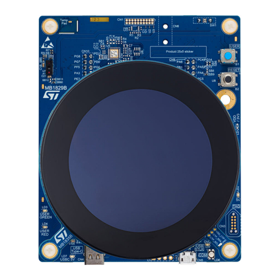
Figure 1.
STM32U5A9J-DK top view
Pictures are not contractual.
UM2967 - Rev 1 - February 2023
For further information contact your local STMicroelectronics sales office.
®
®
‑M33 core with Arm
Cortex
®
HS, Octo‑SPI flash memory device, Hexadeca‑SPI PSRAM memory device, eMMC flash
Discovery kit with STM32U5A9NJ MCU
®
®
TrustZone
.
™
MMU.
STM32CubeU5
MCU Package, which provides an
Figure 2.
STM32U5A9J-DK bottom view
UM2967
User manual
STM32U5A9NJH6Q
®
interface and
www.st.com
Advertisement
Table of Contents

Related Manuals for ST UM2967


Summary of Contents for ST UM2967
-
Page 1: Figure 1. Stm32U5A9J-Dk Top View
STM32 comprehensive software HAL library as well as various software examples. Figure 1. STM32U5A9J-DK top view Figure 2. STM32U5A9J-DK bottom view Pictures are not contractual. UM2967 - Rev 1 - February 2023 www.st.com For further information contact your local STMicroelectronics sales office. -
Page 2: Features
MIPI10 ™ – Tag‑Connect 10‑pin footprint • Flexible power-supply options: ST-LINK USB V , USB connector, or external sources • On-board STLINK-V3E debugger/programmer with USB re-enumeration capability: mass storage, Virtual COM port, and debug port • Comprehensive free software libraries and examples available with the... -
Page 3: Ordering Information
MCU series in STM32 32-bit Arm Cortex MCUs STM32U5 Series MCU product line in the series STM32U599/5A9 product line STM32 flash memory size: 4 Mbytes • J for 4 Mbytes Discovery kit Discovery kit UM2967 - Rev 1 page 3/68... -
Page 4: Development Environment
Windows is a trademark of the Microsoft group of companies. Development toolchains ® ® • IAR Systems - IAR Embedded Workbench ® • Keil - MDK-ARM • STMicroelectronics - STM32CubeIDE 1. On Windows ® only. UM2967 - Rev 1 page 4/68... -
Page 5: Laser Consideration
The laser output power must not be increased by any means and no optics used to focus the laser beam. Figure 3 shows the warning label for Class 1 laser products. Figure 3. Class 1 laser product label UM2967 - Rev 1 page 5/68... -
Page 6: Conventions
SBx connections closed by 0 Ω resistor Solder bridge SBx OFF SBx connections left open Resistor Rx ON Resistor soldered Resistor Rx OFF Resistor not soldered Capacitor Cx ON Capacitor soldered Capacitor Cx OFF Capacitor not soldered UM2967 - Rev 1 page 6/68... -
Page 7: Quick Start
STLINK-V3E product, with new functionalities, bug fixes, support for new microcontroller families, it is recommended to visit the www.st.com website, before starting to use the STM32U5A9J-DK Discovery kit and periodically, to stay up-to-date with the latest firmware version. UM2967 - Rev 1 page 7/68... -
Page 8: Hardware Layout And Configuration
4-Gbyte eMMC flash SDMMC1 I2C4 Stereo jack with microphone Switch Boot0 Boot0 20-pin audio MEMs MDF/ADF connector ADC124 x 7 USART3 Timers, PIOs LPUART1 SAI 1/2 SPI 2/3 I2C 1/2/6 SDMMC2 Expansion connectors UM2967 - Rev 1 page 8/68... -
Page 9: Product Layout (Top And Bottom)
(LD2) 10-pin TAG-connect footprint User green (CN3) LED (LD3) OVC LED User red (LD5) LED (LD4) COM LED (LD6) ® USBC 5V USB Type-C STLINK-V3E USB STLK LED (LD7) connector (CN4) (U10) connector (CN5) UM2967 - Rev 1 page 9/68... -
Page 10: Figure 6. Stm32U5A9J-Dk Bottom Layout View
Octo-SPI flash (U22) IDD 3V3 header (JP1) header (JP2) Power source header (JP4) IDD_MCU header (JP3) MIPI10 connector (CN11) TNRST header (JP5) STLK_NRST Hexadeca-SPI STM32U5A9 eMMC flash header (JP6) PSRAM (U34) MCU (U25) (U26) UM2967 - Rev 1 page 10/68... -
Page 11: Mechanical Drawings
UM2967 Mechanical drawings Mechanical drawings All measurements are in millimeters 7.3.1 Main board top Figure 7. MB1829 top UM2967 - Rev 1 page 11/68... -
Page 12: Main Board Bottom
UM2967 Mechanical drawings 7.3.2 Main board bottom Figure 8. MB1829 bottom UM2967 - Rev 1 page 12/68... -
Page 13: Daughterboard Top
UM2967 Mechanical drawings 7.3.3 Daughterboard top Figure 9. MB1835 top UM2967 - Rev 1 page 13/68... -
Page 14: Daughterboard Bottom
UM2967 Mechanical drawings 7.3.4 Daughterboard bottom Figure 10. MB1835 bottom UM2967 - Rev 1 page 14/68... -
Page 15: Embedded Stlink-V3E
The STM32U5A9J-DK product can be powered from the ST-LINK USB connector (CN5), but the host PC might provide only 100 mA to the ST-LINK circuit until the end of the USB enumeration. The LD3985 LDO (U13) supplies 3.3 V to STLINK-V3E with up to 5.5 V recommended input voltage. Then, the STLINK-V3E requires a 500 mA current to the host PC. -
Page 16: Stlink-V3E Deactivation (Reset Mode)
Table 4). Programming, debugging, and monitoring through ST-LINK are impossible in this Reset state, where all STLINK-V3E PIOs are in high impedance. Attention: The Reset mode is useful to connect an external probe to MIPI10/STDC14 debug (CN11) or TAG (CN3) connector for embedded STM32U5A9NJ debug. -
Page 17: Drivers
STLINK-V3E supports the Virtual COM port (VCP) by default. Communication between the target MCU and ST-LINK MCU is enabled on USART1 (PA9/PA10). The Virtual COM port settings are 115200 bps, 8-bit data, no parity, 1 stop bit, and no flow control. -
Page 18: Power Supply
5V_UCPD, up to 3.0 A: power the board from a 1.5 or 3.0 A compatible USB Host port or USB charger and check the 5 V power supply voltage tolerance fits with the application. UM2967 - Rev 1 page 18/68... -
Page 19: Figure 15. Power Diagram
VREFP 1V8_f up to 650 up to 50 MB1835B To peripherals ( Ext. Conn. + DSI_V3 + SB ON VDD_LCD ST-LINK) 35 mA DSI_V3 => Up to 150 mA up to 100 SB ON => 0 mA 3V3_LCD TPS76301 To peripherals... -
Page 20: Power Source Selection
The USB ST-LINK CN5 connector can power the STM32U5A9J-DK Discovery kit, but the host PC only provides 100 mA to the ST-LINK circuit until the end of USB enumeration. At the end of the USB enumeration, the STM32U5A9J-DK Discovery kit requires a 500 mA current from the host PC. -
Page 21: Chgr
CHGR Figure 17 shows 5 V DC power from CHGR on JP4, with a Power source connected to USB ST-LINK (CN5) and without any current protection. Thus, if the STM32U5A9J-DK Discovery kit is powered by a USB PC port, debug features are available, but with the risk to damage the PC. -
Page 22: E5V
IDD 3V3 (JP1): Current from 3V3_SMPS to 3V3 power supply (VDDUSB of MCU and 3V3 of peripherals) • IDD (JP2): Current from VDDMCU_SMPS to VDD peripheral power supply (VDD is going only to peripherals) • IDD MCU (JP3): Current from VDDMCU_SMPS to VDD_MCU (only to the MCU) UM2967 - Rev 1 page 22/68... -
Page 23: Vdd_Mcu
9.3.3 Analog power supplies VDDA is the external analog power supply for ADC converters, DAC converters, voltage reference buffers, operational amplifiers, and comparators. It is connected to VDD_MCU by default, through a ferrite bead. UM2967 - Rev 1 page 23/68... -
Page 24: Other Peripheral Power
LEDs. A dedicated TPS62140 SMPS provides the 3V3 power rail, to be compatible with the current design and peripherals. STLINK-V3E is powered by the 3V3_STLK supply (LD3985 LDO) from different 5V sources. 5.5 V is the maximum recommended continuous input voltage, up to 6.5 V peak AMR. UM2967 - Rev 1 page 24/68... -
Page 25: Clock Sources
STLINK-V3E, but the clock tree might be adapted, and some features might be unavailable). The LSE might be replaced by internal LSI use, but the clock tree might be adapted, and some features might be unavailable. UM2967 - Rev 1 page 25/68... -
Page 26: Boot Options
SW1 is located on the bottom side of the board due to mechanical constraints. For specific purposes, the switch might be moved on top when CN1 is not used or replaced with a standard 3-pole header with a jumper. Figure 21. BOOT0 default configuration, set on “0” (SW1) UM2967 - Rev 1 page 26/68... -
Page 27: Board Functions
LCD module board. The DSI_TOUCH_INT PIO (PE8, active low) manages the touchscreen interrupt function, to synchronize touch- panel activation with Host. It might also wake up the MCU from standby/shutdown modes. UM2967 - Rev 1 page 27/68... -
Page 28: Display And Dsi_V3 I/O Interface
Add a 2.7 kΩ resistor on R5 of MB1232A. • Use the free spacer/screw and pillar to attach MB1232A onto MB1829 for strong mechanical plugging. Note: MB1232A-01 is part of B-LCDAD-HDMI1 product version 1. UM2967 - Rev 1 page 28/68... -
Page 29: Usb Type-C (High Speed, Sink Only)
Current load lines and check the 7V maximum overvoltage V protection is fitting your need). The TCPP01-M12, associated with a power switch, is used to protect STM32U5A9J-DK from ESD and USB V over-voltage (6.5 V typical, up to 7 V). UM2967 - Rev 1 page 29/68... -
Page 30: Usb 2.0 High-Speed Interface
480 Mbit/s. This allows limited time to transfer data into the embedded 4‑Gbyte eMMC flash memory for example. 12.2.3 ® USB Type-C function interface ® Table 11. USB Type-C function interface Configuration PE12 FLT (UCPD.FLT) DBn (UCPD.DBn) ADC1 (UCPD.ADC1) - optionally used UM2967 - Rev 1 page 30/68... -
Page 31: Hexadeca-Spi Psram Memory
IO5 (HEXASPI1.IO5) IO6 (HEXASPI1.IO6) IO7 (HEXASPI1.IO7) NCLK - not used/not accessible DQS1 (HEXASPI1.DQS1) IO8 (HEXASPI1.IO8) PI10 IO9 (HEXASPI1.IO9) PI11 IO10 (HEXASPI1.IO10) PI12 IO11 (HEXASPI1.IO11) PI13 IO12 (HEXASPI1.IO12) PI14 IO13 (HEXASPI1.IO13) PI15 IO14 (HEXASPI1.IO14) IO15 (HEXASPI1.IO15) UM2967 - Rev 1 page 31/68... -
Page 32: Octo-Spi Flash Memory
The MB1829 main board supports at least the following modes: DDR mode at 40 MHz (no HSLV PIO mode) or SDR mode at 80 MHz in HS200 mode (with HSLV PIO mode). The eMMC_RSTn (PH6, active low) is the reset for eMMC. UM2967 - Rev 1 page 32/68... -
Page 33: Audio Codec (Not Used)
MDF and ADF interfaces are available through one clock and two data wires. PE10, PF4, and PF3 PIOs can manage up to four MEMS microphones. PE13 (Audio_MEMS_LED) is a control PIO to light a LED. UM2967 - Rev 1 page 33/68... -
Page 34: Time-Of-Flight Sensor
Section 4 for a detailed explanation. The VL53L5CXV0GC/1 is a state‑of‑the‑art, Time‑of‑Flight (ToF), laser‑ranging sensor enhancing the ST FlightSense product family. It can be used for gesture control as well as for accurate distance measurements. The device uses an analog power supply of 3.3 V, which starts after the 1.8 V digital supply. The ToF sensor (U7) is managed with an I C shared with a temperature sensor (up to 400 kHz), an LPN control, and an interrupt line. -
Page 35: Temperature Sensor
If the user wants to use PC13 as an output, it is recommended to disconnect the serial resistor (or change it to 220 Ω for example) to protect it from unwanted short circuits to VDD through the button. UM2967 - Rev 1 page 35/68... -
Page 36: Reset Button And Reset Function
USER_RED LED LED_RED, PE1 Lit when STLK overcurrent ST-LINK Overcurrent LED (OVC) detected Red, green, or orange ST-LINK COM LED Lit according to ST-LINK status ® Lit when USB Type-C Green USBC Power LED connected and powered from source 1. LD1 function is not populated by default. -
Page 37: Swd Debug/Program/Trace And Jtag/Usart
5V on pin 5, or simply remove the dedicated solder bridge from PCB, or find a way to disconnect the 5V signal from your tool. Warning: The CN11 and CN3 connectors are exclusives, use only one at the same time to avoid conflict. UM2967 - Rev 1 page 37/68... -
Page 38: Swd, Swo, Jtag, And Usart I/O Interface
Put the embedded STLINK-V3E in Reset mode: Move the TRNST jumper (JP5) on the STLK_NRST header (JP6), no data transfer is possible from USB ST-LINK. This allows using either CN11 or CN3 without the risk of signals conflict with STLINK-V3E on any interface. -
Page 39: Connectors
(front view) (CN4) ® The related pinout for the USB Type-C connector is detailed in Figure 24 Table ® Figure 24. USB Type-C connector pinout (CN4) TX1+ TX1- SBU1 RX2- RX2+ RX1+ RX1- SBU2 TX2- TX2+ UM2967 - Rev 1 page 39/68... -
Page 40: Debug Connector (Cn11)
MIPI10 10-pin connector on the 14‑pin footprint (default configuration) • STDC14 14‑pin connector (option) Attention: Before using CN11, check specific constraints in Section 12.14 SWD debug/program/trace and JTAG/USART. 13.2.1 MIPI10 debug connector (default configuration) Figure 25. MIPI10 debug connector (CN11) UM2967 - Rev 1 page 40/68... -
Page 41: Stdc14 Debug Connector (Option)
Pins 1, 2, 13, and 14 belong to the STDC14 footprint and are not accessible with a MIPI10 compatible probe. 13.2.2 STDC14 debug connector (option) The STDC14 debug connector might be implemented, depending on supported tools, for easy interface with ST tools ecosystem. Figure 26. -
Page 42: Tag Connector (Cn3)
TAG connector (CN3) Figure 28. TC2050-IDC-NL cable Table 25. TAG connector pinout Description Signal assignment Description Signal assignment number number VDD (1.8V) NRST T_NRST (PG10) SWDIO/JTMS T.SWDIO (PA13) JTDI T.JTDI SWCLK/JTCK T.SWCLK (PA14) SWO/JTDO T.SWO (PB3) UM2967 - Rev 1 page 42/68... -
Page 43: Dsi_V3 Display Board Connector (Cn2)
DSI_SPI_CS SPI chip select PB13/ Power output 5V_LCD DSI_SPI_CLK SPI/USART clock PD10 PD4/ DSI_SPI_MOSI SPI/USART data PB10 BLGND DSI_SPI_DCX PD11 SPI data/control BLGND RESERVED 3V3_LCD 3.3 V voltage VDD voltage VDD_LCD reference (1.8 V) UM2967 - Rev 1 page 43/68... -
Page 44: Audio Jack (Not Used) (Cn6)
Note: SAI audio codec and audio jack are not present by default. The 3.5 mm stereo audio jack supports stereo line or headphone outputs and an analog microphone: Figure 30. Audio jack connector (CN6) UM2967 - Rev 1 page 44/68... -
Page 45: Stlink-V3E Usb Micro-B Connector (Cn5)
The USB connector (CN5) is used to interface with STLINK-V3E. It is compatible with USB 2.0 high‑speed transfer data rate. Figure 31. USB Micro-B connector (CN5) 1 2 3 4 5 Table 28. USB Micro-B (CN5) pinout Pin number Description Pin number Description VBUS ID (not used) GND, Shield UM2967 - Rev 1 page 45/68... -
Page 46: Expansion Connectors (Cn9 And Cn10)
TSW-119-08-F-D from SAMTEC 13.7.1 Pin assignment and connectors Figure 32. Female expansion connectors (CN9 and CN10) The pinout of both connectors is summarized in Table 29 Table The bold text describes the default configuration. UM2967 - Rev 1 page 46/68... -
Page 47: Table 29. Connector Pinout (Bottom View) (Cn9)
PF13 PF13 PB12 SPI2_NSS PB12 SPI2 TIM3_CH2 TIM3 PB13/ SPI2_SCK/ PB13/ SPI3_CS/ SPI3/ SPI2/SAI2 PG15 PG15 PD10 SAI2_SCK PD10 LPTIM1_CH1 LPTIM1 PD4/ SPI2_MOSI/ PD4/ SPI3_MOSI/ SPI3/ SPI2/SAI2 PG11 PG11 PD11 SAI2_SD_A PD11 TIM15_CH2 TIM15 UM2967 - Rev 1 page 47/68... -
Page 48: 20-Pin Audio Connector (Not Used) (Cn1)
20‑pin audio connector (CN1) Table 31. 20‑pin audio connector pinout (CN1) Description Assignment Description Assignment number number Ground VDD (1.8V) CCK0 MIC.CCK0 (PF3) SDIN4 MIC.SDIN4 (PE10) SDIN0 MIC.SDIN0 (PF4) Audio_MEMs_LED MEMS_LED (3.3V) (PE13) VDD (1.8V) Ground UM2967 - Rev 1 page 48/68... -
Page 49: Jumpers And Solder Bridges
Set STLINK-V3E in Reset mode (All IOs in high STLK_NRST STLINK-V3E Reset state impedance), no Power from JP4 STLK 1. The default setting is in bold. 2. JP5 and JP6 must not be ON together. UM2967 - Rev 1 page 49/68... -
Page 50: Solder Bridges
Connect SPI_USART_CS to PD8 SPI_USART_CS SB15 connection Let SPI_USART_CS floating Connect SPI_CLK to PD10 SB16 SPI_CLK connection Let SPI_CLK floating Connect SPI_CLK to PB13 SB17 SPI_CLK connection Let SPI_CLK floating Connect SPI_D/CX to PD11 SB18 SPI_D/CX connection UM2967 - Rev 1 page 50/68... - Page 51 Connect VDDUSB to VDD_MCU SB35 VDDUSB connection Isolate VDDUSB from VDD_MCU VDDA is connected to VDD_MCU SB36 VDDA connection VDDA not connected to VDD_MCU Connect VDDUSB to 3V3 SB37 VDDUSB connection Isolate VDDUSB from 3V3 UM2967 - Rev 1 page 51/68...
- Page 52 Connect IOREF (VDD) to CN9 IOREF (VDD) connection SB56 to CN9 Isolate IOREF (VDD) from CN9 UCPD.ADC2 (PF15) is connected to USB-C UCPD.ADC2 (PF15) SB57 connection to USB-C UCPD.ADC2 (PF15) is not connected to USB-C UM2967 - Rev 1 page 52/68...
- Page 53 3V3 is disconnected from the AVDD of the ToF sensor GND is connected to TAG pin 5 GND connection to TAG SB61 connector pin 5 GND is disconnected from TAG pin 5 1. The default setting is in bold. UM2967 - Rev 1 page 53/68...
-
Page 54: Stm32U5A9Njh6Q Gpio And Pin Assignment
Pin 26 of CN9 PB11 USART3 _RX Exp. conn. USART3 Pin 24 of CN9 PB12 SPI2 _NSS Exp. conn. SPI2 Pin 17 of CN10 PB13 SPI2 _SCK Exp. conn. SPI2 DSI_V3 connector Pin 15 of CN10 UM2967 - Rev 1 page 54/68... - Page 55 TP31 PD15 TIM4_CH4 Exp. conn. TIMER Pin 28 of CN10 LED_GREEN USER LED LED_RED USER LED SAI1 for Audio Codec and SAI1.MCLK_A SAI1_MCLK Pin 1 of CN10 Exp. conn. SAI1.SD_B SAI1 for Audio Codec UM2967 - Rev 1 page 55/68...
- Page 56 VBUS_SENSE USB Type-C PG2 (free) TP26 PG3 (free) TP30 PG4 (free) TP27 PG5 (free) TP29 PG6 (free) TP28 LPUART1_TX Exp. conn. LPUART1 Pin 36 of CN10 LPUART1_RX Exp. conn. LPUART1 Pin 38 of CN10 UM2967 - Rev 1 page 56/68...
- Page 57 Hexadeca-SPI HEXASPI1.DQS0 Hexadeca-SPI HEXASPI1.CLK Hexadeca-SPI PI4 (free) Not accessible DSI_PWR_ON DSI_V3 connector DSI_BL_CTRL DSI_V3 connector DSI_SWIRE DSI_V3 connector HEXASPI1.DQS1 Hexadeca-SPI HEXASPI1.IO8 Hexadeca-SPI PI10 HEXASPI1.IO9 Hexadeca-SPI PI11 HEXASPI1.IO10 Hexadeca-SPI PI12 HEXASPI1.IO11 Hexadeca-SPI PI13 HEXASPI1.IO12 Hexadeca-SPI UM2967 - Rev 1 page 57/68...
- Page 58 Power VSSA AGND AGND VREFP VDDA Power VREFM AGND AGND VDDUSB Power VDD11USB Power VDDDSI VDD_MCU Power VDD11DSI Power VSSDSI DSI GND VDDSMPS Power VLXSMPS SMPS VLX Power VSSSMPS SMPS GND VBAT VDD_MCU Power UM2967 - Rev 1 page 58/68...
-
Page 59: Stm32U5A9J-Dk Product Information
B01. The second line shows the board serial number used for traceability. Parts marked as “ES” or “E” are not yet qualified and therefore not approved for use in production. ST is not responsible for any consequences resulting from such use. In no event will ST be liable for the customer using any of these engineering samples in production. -
Page 60: Board Revision History
Board change description Board limitations MB1829 MB1829-U5A9NJQ-B01 Initial revision The C2 and C3 silkscreen are inverted by the PCB manufacturer MB1835 MB1835-VDD1V8-B01 Initial revision (error present in original MB1835B Gerber files corrected by PCB manufacturer). UM2967 - Rev 1 page 60/68... -
Page 61: Federal Communications Commission (Fcc) And Innovation, Science And Economic
750 Canyon Drive | Suite 300 | Coppell, Texas 75019 Telephone: +1 972-466-7845 17.2 ISED Compliance Statement ISED Canada ICES-003 Compliance Label: CAN ICES-3 (B) / NMB-3 (B). Étiquette de conformité à la NMB-003 d'ISDE Canada: CAN ICES-3 (B) / NMB-3 (B). UM2967 - Rev 1 page 61/68... -
Page 62: Revision History
UM2967 Revision history Table 37. Document revision history Date Revision Changes 10-Feb-2023 Initial release. UM2967 - Rev 1 page 62/68... -
Page 63: Table Of Contents
Analog power supplies ........... 23 UM2967 - Rev 1... - Page 64 STLINK-V3E USB Micro-B connector (CN5) ........45 UM2967 - Rev 1...
- Page 65 List of figures................67 UM2967 - Rev 1...
-
Page 66: List Of Tables
Document revision history ............. 62 UM2967 - Rev 1... -
Page 67: List Of Figures
20‑pin audio connector (CN1) ............48 UM2967 - Rev 1... - Page 68 ST’s terms and conditions of sale in place at the time of order acknowledgment. Purchasers are solely responsible for the choice, selection, and use of ST products and ST assumes no liability for application assistance or the design of purchasers’...
Need help?
Do you have a question about the UM2967 and is the answer not in the manual?
Questions and answers