Table of Contents
Advertisement
Quick Links
ISO 9001:2015
Certified
TIMTER
TM
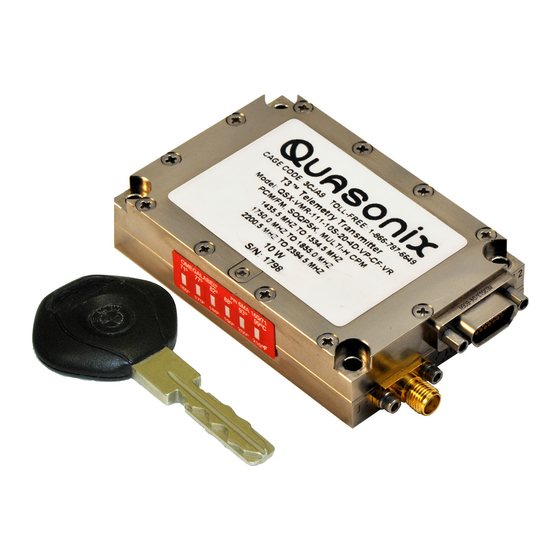
Multi-mode Digital Telemetry Transmitter
Installation and Operation Manual
Quasonix, Inc.
6025 Schumacher Park Dr.
West Chester, OH 45069
23 February 2021
Revision 3.9.2
Specifications subject to change without notice.
All Quasonix transmitter products are under U.S. Department of Commerce jurisdiction and categorized
as EAR99; not covered by ITAR.
No part of the document may be circulated, quoted, or reproduced for distribution without prior written approval from
Quasonix, Inc.
Copyright Quasonix, Inc., All Rights Reserved.
Advertisement
Table of Contents

Related Manuals for Quasonix TIMTER QSX-V Series

Summary of Contents for Quasonix TIMTER QSX-V Series
- Page 1 Revision 3.9.2 Specifications subject to change without notice. All Quasonix transmitter products are under U.S. Department of Commerce jurisdiction and categorized as EAR99; not covered by ITAR. No part of the document may be circulated, quoted, or reproduced for distribution without prior written approval from Quasonix, Inc.
-
Page 2: Table Of Contents
Clock Generator Output Option – CG ................... 13 1.3.18 Dual Power Option – DP ....................... 13 1.3.19 Digital Switch Box Option – DSWBX ..................13 1.3.20 Ethernet Payload Capability – EN ..................13 1.3.21 Analog Frequency Modulation – FM ..................14 1.3.22 Quasonix, Inc. - Page 3 Recall Holdoff Option – RH ....................17 1.3.44 Randomizer Output Option – RN ..................17 1.3.45 Spacecraft Tracking and Data Network Option – STDN ............17 1.3.46 Variable FIFO Depth Option – VF ..................17 1.3.47 Variable Power Option – VP ....................17 1.3.48 Quasonix, Inc.
- Page 4 Baseband Clock – BBCK ..................59 4.2.1.1.2 Clock Free Bit Rate – BR ..................60 4.2.1.1.3 4.2.1.1.4 Baseband Interface Type - BT ................. 62 Convolutional Encoder – CC ................... 62 4.2.1.1.5 Clock Generator Source Select Command – CG ............ 62 4.2.1.1.6 Quasonix, Inc.
- Page 5 4.2.1.1.20 External Device Polarity Invert Command – XDP ..........73 4.2.1.1.21 RF Output Notes ..........................74 Troubleshooting the RF on a Quasonix Transmitter ..............74 Performance Specifications ......................... 77 RF Output ..........................77 Electrical Current ........................77 Environmental Specifications..................... 78 6.3.1...
- Page 6 Appendix C – Understanding Clock/Data, AC, and BR ..............100 Appendix D – Acronym List ......................102 List of Figures Figure 1: Quasonix Part Number Construction Description ................1 Figure 2: FPCM Signal on Oscilloscope ..................... 10 Figure 3: CCSDS 131.0-B-1 Rendering of Basic Convolutional Encoder Diagram ........12 Figure 4: Fan-cooled Heat Sink and Power Supply ..................
- Page 7 Table 9: RF Output Power Codes ......................... 9 Table 10: Package Codes ..........................9 Table 11: Standard Data Bit Rates and Rate Adaptation Compared to Clock Free Data Bit Rates ..13 Table 12: Standard Bit Rates Compared to Low/High Rate Options ............15 Quasonix, Inc.
- Page 8 Table 16: TIMTER™ EMI Compliance ......................78 Table 17: Carrier Frequencies (MHz) ......................79 Table 18: Transmitter BER Specifications with Quasonix Demodulator ............. 81 Table 19: K and m Values per Waveform ....................82 Table 20: Random Vibration Spectrum ....................... 88 Table 21: Transmitter Priority of CS, CF, BR, and AC When RF is On ............
-
Page 9: Introduction
The type of features and modes installed in each unit are identified in the model number, as depicted in Figure 1. Package field codes are listed in Table 10. For questions about specific packages, please contact Quasonix. Transmitter Part Numbering Example... - Page 10 Adapter plate for 2.5” x 3.5” footprint – Include this hardware accessory with order • Request non standard baud rate for serial control • Quasonix interpretation of IRIG 106-17 Appendix 2-C serial control protocol • Convolutional encoder (includes NRZ-M encoding) (k=7 rate 1/2) •...
-
Page 11: Table 1: Model Configuration Example
Refer to Table 13 in section 4.2.1 for detailed descriptions of each option. Due to input connector pin count limitations, certain combinations of options are not available. Please contact Quasonix for support in ordering TIMTER™ options or for information regarding upgrades to TIMTER™ units that you may already own. -
Page 12: Part Number Field Codes
1435.5 MHz 1534.5 MHz 1450.5 MHz 0.5 MHz 10 W 4400.0 MHz 4950.0 MHz C, Mid C, and 4400.0 MHz 4950.0 MHz 4620.0 MHz 0.5 MHz 18 W Euro Mid C 5091.0 MHz 5150.0 MHz 5150.0 MHz 5250.0 MHz Quasonix, Inc. - Page 13 Euro Mid C 5150.0 MHz 5250.0 MHz *Note: Currently the MA option enables below Lower S band frequencies for use in space operations and space research. Refer to the MA option in section 1.3.34 for additional information or contact Quasonix. Quasonix, Inc.
-
Page 14: Clock And Data Interface
TTL 75 ohms and RS-422 (terminated 120 ohms differential) Tri-mode – Selectable between TTL (terminated 75 ohms to ground), TTL 75 ohms TTL (terminated 10k ohms to ground), and RS-422 (terminated 120 ohms differential) LVDS (Low Voltage Differential Signal) LVDS Quasonix, Inc. -
Page 15: Serial Control Interface
Table 4: Serial Control Interface Codes Serial Control Serial Control Interface Interface Code LVTTL; 57,600 baud rate RS-232; 57,600 baud rate TTL; 57,600 baud rate RS-422; 57,600 baud rate RS-422; 57,600 baud rate, 120 ohms differential, even when unit is powered off Quasonix, Inc. -
Page 16: Artm Tier 0 (Pcm/Fm)
Table 7: ARTM Tier II Codes Part Number Code Multi-h CPM (ARTM Tier II) Absent Present 1.3.7 Legacy Legacy modes include BPSK, QPSK, and OQPSK. Legacy codes are listed in Table 8. Table 8: Legacy Codes Part Number Code Legacy Modes Absent Present Quasonix, Inc. -
Page 17: Rf Output Power
Packages Package field codes are listed in Table 10. Detailed information for packages other than 04AB is located in the TIMTER™ Transmitter Packages document, available at the Quasonix web site. For questions about specific packages, please contact Quasonix. Table 10: Package Codes TIMTER™... -
Page 18: Automatic Carrier Wave Output Option - Ac
TIMTER™ Multi-mode Digital Telemetry Transmitter Transmitter weight may vary depending on packages and applications. For information about the weight of a particular transmitter, please contact Quasonix. 1.3.10 Automatic Carrier Wave Output Option – AC This option allows the TIMTER to transmit a carrier wave when the clock input is absent, which would normally cause the RF output to be turned off. -
Page 19: Adapter Plate - Ap
0-8 follows the BR option request. Corresponding values are as follows: 0 = 57600 (Standard default for all Quasonix transmitters); 1 = 4800; 2 = 9600; 3 = 19200; 4 = 38400; 5 = 56000; 6 = 57600; 7 = 115200; 8 = 230400. -
Page 20: Clock-Free Baseband Interface Option - Cf
External clock (CS 0 Command) is the normal mode: the user supplies clock and data, or in clock-free mode, the user only supplies valid data. Refer to Table 13 for user commands. Quasonix, Inc. -
Page 21: Clock Generator Output Option - Cg
Ethernet physical layers. The maximum transmission rate is 46 Mbps. Use of a transmitter with the –EN option requires a Quasonix RDMS™ receiver to reconstruct the Ethernet data at the receive end. Pre-assembled MDM-9 Male to RJ-45 (T568A standard) cables are available from Molex:... -
Page 22: Analog Frequency Modulation - Fm
This mode of operation is designed for use with a true analog signal, such as NTSC video. By default, the analog FM input is AC coupled, with a low frequency cutoff of less than 15 Hz. Contact Quasonix if you need a DC coupled analog input. -
Page 23: Table 12: Standard Bit Rates Compared To Low/High Rate Options
CCSDS randomizer, if LDPC is enabled. Adding this option automatically enables the existing LD option. The IRIG standard calls out six variants of LDPC codes—all combinations of two different information block sizes (k=4096 bits and k=1024 bits) and three different code rates (r=1/2, r=2/3, and r=4/5). Quasonix, Inc. - Page 24 1.3.40 Parallel Port Frequency Programming Option – PF This option adds a parallel port in the form of an MDM-15 connector for manual frequency tuning. The PF option requires the addition of a Quasonix MDM-9 Accessory Board. Consult Quasonix to order the PF option. Quasonix, Inc.
- Page 25 This option adds a parallel port in the form of an MDM-15 connector for manual mode selection. The PM option requires the addition of a Quasonix MDM-9 Accessory Board. Consult Quasonix to order the PM option. 1.3.42 Hardware Preset Option – PS (PS2, PS4, PS8, or PS16) The TIMTER™...
-
Page 26: Wide Input Voltage Range Option - Wv
Note: The WV option is not supported on 25 W S-band and 20 W L/C or S/C-band transmitters. 1.3.50 External Device Control – XD This option lets the user control the state and operation of the new TTL output pins on the switchbox interface connector. Refer to section 4.2.1 for command descriptions. Quasonix, Inc. -
Page 27: Accessories
TIMTER™ Multi-mode Digital Telemetry Transmitter 2 Accessories Quasonix offers a number of optional accessories for TIMTER™, including a fan-cooled heat sink, a 2.5” x 3.5” adapter plate, pre-wired mating MDM-15 connectors, complete MDM-15 cable assemblies, a ruggedized handheld programmer, and a USB to serial converter cable. Contact Quasonix for pricing and availability of TIMTER™... -
Page 28: Transmitter-Powered Heat Sink (For Airborne Applications)
The heat sink is shown mounted on a standard 04AB TIMTER™ in Figure 7 and mounted on a larger 07AE TIMTER™ in Figure 8. The pigtail cable connects to any TIMTER™, regardless of MDM-15 gender, by plugging the pigtail into either the male or female connector, as shown in Figure 9 and Figure 10. Quasonix, Inc. -
Page 29: Figure 7: Transmitter-Powered Heat Sink Mounted On An 04Ab Package
TIMTER™ Multi-mode Digital Telemetry Transmitter Figure 7: Transmitter-powered Heat Sink Mounted on an 04AB Package Figure 8: Transmitter-powered Heat Sink Mounted on a 07AE Package Quasonix, Inc. -
Page 30: Adapter Plate
Figure 11: Adapter Plate 2.4 Pre-wired MDM-15 for RS-422 Units Part Number: QSX-AC-MDM15-36-PIN An MDM-15 connector with 36” color-coded pigtail cables for connecting to transmitters with the RS-422 clock and data baseband interface is shown in Figure 12. Quasonix, Inc. -
Page 31: Pre-Wired Mdm-15 For Ttl Units
2.5 Pre-wired MDM-15 for TTL Units Part Number: QSX-AC-MDM15-36-SOCK Quasonix offers an MDM-15 connector with 36” color-coded pigtail cables for connecting to transmitters with the TTL clock and data baseband interface. Figure 13: Pre-wired MDM-15 with 36” Pigtails for TTL 2.6 MDM-15 Wiring Harness for RS-422 Units... -
Page 32: Wiring Harness For Ttl Units
2.7 MDM-15 Wiring Harness for TTL Units Part Number: QSX-AC-MDM15-HARNESS-SOCK Quasonix offers an MDM-15 wiring harness for connecting to transmitters with TTL clock and data baseband interface. It includes banana plugs for power and ground, BNC connectors for clock and data, and a DB-9 connector for serial control and is 35 to 36 inches long depending on the connectors. -
Page 33: Usb To Serial Converter Cable
TIMTER™ Multi-mode Digital Telemetry Transmitter The 2 Generation Handheld Programmer is an ultra-rugged Pocket PC with custom Quasonix software that allows the user to configure transmitters through its serial interface directly in the field. The programmer is shown in Figure Figure 16: Ruggedized Handheld Programmer 2.9 USB to Serial Converter Cable... -
Page 34: Nd Generation Digital Switch Box
The transmitter which will use the switch box requires the P9 option when ordering to ensure an MDM-9 port is installed. If you already own a Quasonix transmitter with an old switch box, the digital switch box can be swapped for the old one seamlessly. -
Page 35: Installation Instructions
The standard 4.2 cubic inch TIMTER™ (04AB package) is designed to be mounted by four (4) 6-32 screws through the holes in the four corners, as depicted in Figure 20. Drawings for all TIMTER™ packages are located on the Quasonix web site. Figure 19: 4.2 in3 TIMTER™... -
Page 36: Figure 20: Outline Drawing, Timter™ 04Ab Telemetry Transmitter
TIMTER™ Multi-mode Digital Telemetry Transmitter Figure 20: Outline Drawing, TIMTER™ 04AB Telemetry Transmitter Quasonix, Inc. -
Page 37: Thermal
Quasonix offers several types of integrated and add-on heat sinks (refer to Section 0). Please contact Quasonix for heat sink recommendations for your particular TIMTER™ transmitter. -
Page 38: Figure 21: Example Quasonix Pinout Drawing
Most browsers allow you to right click on the link and determine how to open it or print it, regardless of the default setting. Figure 21: Example Quasonix Pinout Drawing The data is sampled on the falling edge of the clock, as shown in Figure 22. -
Page 39: Figure 22: Baseband Signal Timing
TIMTER™ Multi-mode Digital Telemetry Transmitter Figure 22: Baseband Signal Timing Quasonix, Inc. -
Page 40: Operating Instructions
2nd Generation Switch Box Notes If a Quasonix 2nd Generation Digital Switch Box is attached to the transmitter, and the digital switch box option is present (check the part/model number of the transmitter for DSWBX), all changes made to mode, frequency, or LDPC selections on the transmitter are also updated immediately on the Switch Box. -
Page 41: Command Set: Standard And Optional Commands
TIMTER™ Multi-mode Digital Telemetry Transmitter Quasonix Multi-Mode Digital Transmitter Customer Part # = QSX-xxx-xx-xx… Customer Name = Quasonix Customer Contract # = 999999-9 TX Serial # = 1001 Hardware Rev: A PA Rev: F PA Serial #: 1001 PA Model #: XMTR-PAM-10-F-SCPA... -
Page 42: Table 13: Standard And Optional User Commands
CS and/or DS as 1 from a saved configuration is by executing the RC command. Note: All user commands do not apply to all transmitters. Command availability varies depending on the options ordered and any project specific customization applied. Questions? Please call Quasonix for assistance. Table 13: Standard and Optional User Commands... - Page 43 With the auxiliary input active, the unit automatically switches to clock-free operation (CF 0). Examples: Report the current value of AI AI 1 Enable the aux input AI 0 Disable the aux input Quasonix, Inc.
- Page 44 Bit rate must be below 35 Mbps to use automatic bit rate detection Examples: Report the bit rate BR 5 Set the bit rate to 5 Mbps BR A Set the bit rate automatically Refer to section 4.2.1.1.3 for related BR command detail Quasonix, Inc.
- Page 45 Report or set the clock free state CF 1 Examples: Report the clock free state CF 0 Unit uses its internal bit sync (internally synthesized) CF 1 Unit uses its externally applied clock Also refer to Appendix C – Understanding Clock/Data, AC, and BR Quasonix, Inc.
- Page 46 CP 1 Set clock polarity to inverted CP A Set clock polarity to auto; Automatically selects the most reliable clock edge Current Preset Reports the currently selected Standard CR 0 Read software preset being used by the transmitter Quasonix, Inc.
- Page 47 Report the differential encoding setting DE 0 Set differential encoding DE 1 Set differential encoding DIOR Display I/O Displays I/O addresses of Standard Register machine registers to make it Addresses easier to debug Example: DIOR Displays I/O addresses Quasonix, Inc.
- Page 48 Read Frequency Returns current value of mode PF, PM, or Plug and frequency from a switch box DSWBX Frequency Plug Displays the frequency plug PF, PM, or Debugs (switch box) debugs with the DSWBX current state for each channel Quasonix, Inc.
- Page 49 If the FO option is present, the resolution is 1 Hz (0.000001 MHz). Examples: Display the current frequency FR ? Display allowed frequency ranges FR 1436.5 Set frequency to 1436.5 MHz Refer to section 4.2.1.1.8 for related FR command detail Quasonix, Inc.
- Page 50 HP 31 Set high power to 31 HP Max Set high power to the highest allowable value for the unit HP Min Set high power to the minimum allowable value for the unit eXtended Help Displays a full list of available Standard commands Quasonix, Inc.
- Page 51 Valid range is 0.002 MHz – 46.0 MHz for most transmitters; some legacy transmitters 0.002 MHz – 28.0 MHz Observes same bit rate limits as HR/LR cmds (PCM/FM half) Refer to section 4.2.1.1.9 for additional IC command detail Quasonix, Inc.
- Page 52 ID USER AA55 Set internal data pattern to 0xAA55 In SOQPSK mode, ID USER 5555 or ID USER AAAA will result in an unmodulated carrier, at the nominal carrier frequency. Internal Model Display the internal model Standard Number number for the transmitter Quasonix, Inc.
- Page 53 I and Q data when the data source is set to internal; if enabled, the ID and QD commands set the two data patterns Examples: Show the current state IQ 1 Enable independent I/Q data IQ 0 Disable the independent I/Q data Quasonix, Inc.
- Page 54 IS command detail List Lists the stored configurations on Standard Configurations the unit If a configuration number is supplied, then the saved parameters for that configuration are displayed. Examples: List all internal saved configurations LC 7 Show configuration 7 details Quasonix, Inc.
- Page 55 LP Min Set low power to the minimum allowable value for the unit Modes Allowed Reports the modes enabled on Standard the transmitter, as determined by the part number Example: Show available modes - PCMFM - SOQPSK - MHCPM Quasonix, Inc.
- Page 56 Set modulation to QPSK MO 6 Carrier only, no modulation MO 7 Set modulation to OQPSK MO 8 Set modulation to UQPSK MO 10 Set modulation to STDN MO 11 Set modulation to SQPN MO 12 Set modulation to Analog_FM Quasonix, Inc.
- Page 57 Control OC 1 Enable Overtemperature Control Refer to section 4.2.1.1.12 for additional OC command detail. Over-the-Air Displays the current baseband Standard Rate and over-the-air bit rate. This information is also displayed on the RFS output. Display over-the-air rate Quasonix, Inc.
- Page 58 Default power level is Full power Query All Displays common device settings Standard in one compact display QT or TE Query Report the temperature in Standard Temperature degrees Celsius Quasonix, Inc.
- Page 59 RF On/Off hardware pin is in the OFF state. Examples: Report the RF output state RF 0 Set RF output OFF RF 1 Set RF output ON Refer to section 4.2.1.1.13 for related RF command detail Quasonix, Inc.
- Page 60 RZ 1 Set RF On/Off polarity to “pin high = on” The default polarity on most Quasonix transmitters is high. The RF On/Off pin is a hard OFF control. No matter what state everything else is in, setting this switch input to the inactive state will turn RF Off.
- Page 61 Examples: Report spectral inversion status SI 0 No inversion SI 1 Invert the spectrum Serial Number Report the serial number for the Standard unit Show Settings Displays most of the common Standard device settings in one compact display Quasonix, Inc.
- Page 62 SW 1 Start the sweep SW 0 Stop the sweep SW 1 2200.5 2394.5 1.0 Sweep channel 1 between 2200.5 MHz and 2394.5 MHz in 1.0 MHz steps Refer to section 4.2.1.1.16 for additional SW command detail Quasonix, Inc.
- Page 63 Examples: Displays current status report settings SY 0 Disables continuous reporting SY 5000 210 Sets status header output once every 210 status updates Refer to section 4.2.1.1.17 for additional SY command detail Quasonix, Inc.
- Page 64 Mode 1, Frequency 1, Frequency 2, and Temperature 1 Temperature Displays the HVA table and/or the Standard Compensation DL table Display Examples: Displays both tables TD ALL Displays both tables TD HVA Displays HVA table only TD DL Displays DL table only Quasonix, Inc.
- Page 65 External Device Report or set the state of the XDC 0 Control extra RS-422 output to use it to control an external device Refer to section 4.2.1.1.18 for additional XDC command detail. Quasonix, Inc.
- Page 66 Available presets depend on the number specified for the unit Values are PS2, PS4, PS8, or PS16 If the PS option is not specified, there is only one (1) hardware preset on the transmitter. Quasonix, Inc.
-
Page 67: Additional Command Set Details
The BBCK command displays the actual current baseband clock rate and source. If Clock Free (CF command) is enabled, and the bit rate (BR command) is fixed at 5.5 Mbps: 1>BBCK BB clock rate = 5.465334 Mbps, src = CF Man (Man indicates the bit rate was set manually) Quasonix, Inc. -
Page 68: Clock Free Bit Rate - Br
Set the clock free bit rate mode to Auto and Disable warning BR A E Set the clock free bit rate mode to Auto and Enable warning Suppose this sequence of commands are issued: 1>BR A CF Bitrate Mode set to Auto Quasonix, Inc. - Page 69 1>BR 6.1 CF Bitrate set to 6.100 Mbps fixed 1>BR CF Bitrate currently 6.100 Mbps (CF Operation NOT Enabled) This example set BR to a fixed rate, but since clock free is not enabled, it is not used. Quasonix, Inc.
-
Page 70: Baseband Interface Type - Bt
4.2.1.1.7 This command is no longer supported. Transmitters with the FO option can be tuned with 1 Hz resolution using the FR (frequency) command. Examples: SOQPSK>FR 2200.2 Freq set to 2200.0 MHz Freq offset set to 0.200000 MHz Quasonix, Inc. -
Page 71: Frequency - Fr
This command can conceivably replace CS, DS, ID, IC, BR, BT, AIR, CF, and EN. This command is standard on all units version 2.409 or greater. Syntax: IS [ds/?/pnxx/XXXX [cs/AUTO/rate]] where ds is data source which can be: ET – external TTL data (if QSX-VxT or -VR enabled) Quasonix, Inc. - Page 72 Actions: ds 0, cs 0, cf 0, br XX.xxx (bt 3, ai 0, and en 0 if needed) If ds = I, then cs MAY be: • Nothing (defaults to internal clock at current IC rate) (displayed) • I for an internal clock at current IC rate (displayed) Quasonix, Inc.
- Page 73 Actions: ds 0, cs 0, ai 1, cf 0 AIR 1 br (en 0 if needed) • AUTO for clock free with BR = auto Actions: ds 0, cs 0, ai 1, cf 0 AIR 1 br a (en 0 if needed) Quasonix, Inc.
-
Page 74: Low Density Parity Check (Ldpc) Command - Ld
LDPC is disabled when a mode change occurs. This is true for all mode changes, *PSK or other modes. There are two exceptions: If preset 0 has LDPC enabled, it stays enabled after a power cycle. Any preset that has LDPC enabled, stays enabled after the preset is recalled (RC command). Quasonix, Inc. -
Page 75: Overtemperature Control - Oc
PA) goes above a set limit stored on the device, and the current power level is over 25, the transmitter automatically starts to back off power in 2 dB steps to a max of 6 dB. Contact Quasonix for the default overtemperature value specific to your transmitter. 4.2.1.1.13 RF Output – RF RF enables or disables the RF power output from the transmitter. -
Page 76: Rf Output State - Rfs
2 – Ignore the switch box (frequency plug) ALWAYS; Only the Terminal interface works until the SC setting changes. The default value is SC 1 if the DSWBX option is present on the transmitter. The default value is SC 2 if the DSWBX option is NOT present on the transmitter. Quasonix, Inc. -
Page 77: Frequency Sweep - Sw
4.2.1.1.17 System Status Command – SY The status reporting period must be > 200 ms or zero (0) to disable. Items in the SY command are defined with the SZ command. The minimum update period is 200 ms (about 5 times per second). Quasonix, Inc. - Page 78 CF Rate because it will track the bit sync rate (exact, if locked) rather than the clock free estimated rate (approximate). This example display shows selected parameters for one channel. CRateB0 CFRate1 Mode 1 Freq 1 Temp 1 (b/s) (b/s) (Hz) 7812666 1852000000 32.5 Quasonix, Inc.
-
Page 79: External Device Control Command - Xdc
0 if XDP is 1 (invert) if FR < XDF then output is 0 if XDP is 0 (no invert) or 1 if XDP is 1 (invert) Examples: XDC ? Help Show the current external device control state Quasonix, Inc. -
Page 80: External Device Channel Command - Xdch
FR < XDF then output is 0 if XDP is 0 (no invert) or 1 if XDP is 1 (invert) Examples: XDF ? Help Show the current external device frequency switching threshold XDF 4430.0 Set the current external device frequency switching threshold to 4430.0 MHz Quasonix, Inc. -
Page 81: External Device Polarity Invert Command - Xdp
0 if XDC = 1 or if XDC = A and current FR >= XDF 1 if XDC = 0 or if XDC = A and current FR < XDF Examples: XDP ? Help Show the current external device polarity invert state Quasonix, Inc. -
Page 82: Rf Output Notes
Examples are auto-carrier (-AC option), clock free (-CF option) and recall-holdoff (-RH option). If the procedure below does not demonstrate the working RF output on the transmitter, please contact Quasonix technical support for further help in resolving the issue. - Page 83 RZ 0 sets the transmitter output to turn ON when the RF On/Off pin is low. Is the output present now? If so, go on to Part 2 below. If not, call Quasonix for technical support. Part 2: Verifying modulation output on frequency with internal data Turn on the transmitter.
- Page 84 (CP) the data polarity (DP), the randomizer (RA), and the differential encoder (DE – normally on for SOQPSK and off for other waveforms) to resolve the sync and bit error rate issues. If you are still having difficulties at this point, then contact Quasonix technical support. Quasonix Technical Support (1-513-942-1287) or email (support@quasonix.com)
-
Page 85: Performance Specifications
L/C band and S/C band 20 mWatt 0.35 amps 0.30 amps L/C band and S/C band 10 Watt 2.2 amps 2.0 amps L/C band and S/C band 18 Watt 3.5 amps 3.2 amps L/S/C band 10 mWatt 0.45 amps 0.40 amps Quasonix, Inc. -
Page 86: Environmental Specifications
This includes electromagnetic interference and compatibility (EMI/EMC) requirements. More specifically, all Quasonix transmitters in the TIMTER™ family (2 cubic inches and above) have been designed to comply with the following requirements of MIL-STD-461G (and MIL-STD-461E and -461F, when those now-obsolete standards have been applied): Table 16: TIMTER™... -
Page 87: Carrier Frequency Tuning
RS103 Radiated Susceptibility, Electric Field Quasonix transmitters have been tested for compliance with these standards approximately annually since 2004. However, such testing is only performed as part of a qualification program, and the test results are the exclusive property of the customer who paid for them. If you need EMI testing on a particular part number, please contact sales@quasonix.com for a quote. - Page 88 S, Mid C, and 2200.5 MHz 2394.5 MHz 2370.5 MHz 0.5 MHz 18 W (with Euro Mid C) 5091.0 MHz 5150.0 MHz 5150.0 MHz 5250.0 MHz Mid C band 5091.0 MHz 5150.0 MHz 5120.0 MHz 0.5 MHz 20 W Quasonix, Inc.
-
Page 89: Carrier Frequency Error
The frequency error is less than ±20 ppm over all combinations of temperature, voltage, and aging (up to five years). 6.6 Bit Error Rate The transmitter meets the following BER limits when tested with the Quasonix’ multi-mode, multi-symbol trellis demodulator. -
Page 90: Modulated Rf Power Spectrum
As noted in the equation above, the mask has a floor at –(55 + 10 log(P)) dBc, and the mask imposes no limit on the spectrum for frequency offsets less than R/m. Representative examples of the transmitted spectrum, with the appropriate mask, are shown in Figure 24, Figure 25, and Figure 26. Quasonix, Inc. -
Page 91: Figure 24: Pcm/Fm (Tier 0) Power Spectral Density With Mask
TIMTER™ Multi-mode Digital Telemetry Transmitter Figure 24: PCM/FM (Tier 0) Power Spectral Density with Mask Figure 25: SOQPSK-TG (Tier I) Power Spectral Density with Mask Quasonix, Inc. -
Page 92: Phase Noise Power Spectrum
TIMTER™ Multi-mode Digital Telemetry Transmitter Figure 26: MULTI-h CPM (Tier II) Power Spectral Density with Mask 6.8 Phase Noise Power Spectrum TIMTER™ phase noise limits are shown in Figure 27. Quasonix, Inc. -
Page 93: Baseplate Temperature
-40°C to +85 °C, while the 20W version is rated from -40°C to +70 °C. 6.10 Vibration and Shock The transmitter is designed and tested to operate normally when subjected to random vibration and shock. The shock and vibe test setup employed by Quasonix is shown in the following figures. Quasonix, Inc. -
Page 94: Figure 28: Vibration / Shock Testing System
TIMTER™ Multi-mode Digital Telemetry Transmitter Figure 28: Vibration / Shock Testing System Figure 29: TIMTER™ Mounted for Z-axis Testing Quasonix, Inc. -
Page 95: Vibration Testing
Figure 30: TIMTER™ Mounted for X-axis Testing Figure 31: TIMTER™ Mounted for Y-axis Testing 6.10.1 Vibration Testing Each transmitter is subjected to the random vibration spectrum depicted in Figure 32 and Table 20 prior to shipment. Figure 32: TIMTER™ Vibration Profile Quasonix, Inc. -
Page 96: Figure 33: Z-Axis Vibration Spectrum
2000 G (RMS) = 19.6 During flight-qualification testing, the unit under test (UUT) was shaken for 30 minutes in each axis. The results are shown in Figure 33, Figure 34, and Figure 35. Figure 33: Z-axis Vibration Spectrum Quasonix, Inc. -
Page 97: Figure 34: Y-Axis Vibration Spectrum
TIMTER™ Multi-mode Digital Telemetry Transmitter Figure 34: Y-axis Vibration Spectrum Figure 35: X-axis Vibration Spectrum Quasonix, Inc. -
Page 98: Shock Testing
Application: Three (3) shocks in each direction of the three (3) orthogonal axes both positive and negative, for 18 shocks total The plots of the positive and negative pulses in each of the three axes are shown in the following figures: Figure 36: Shock Pulse, Z-axis Positive Quasonix, Inc. -
Page 99: Figure 37: Shock Pulse, Z-Axis Negative
TIMTER™ Multi-mode Digital Telemetry Transmitter Figure 37: Shock Pulse, Z-axis Negative Figure 38: Shock Pulse, Y-axis Positive Quasonix, Inc. -
Page 100: Figure 39: Shock Pulse, Y-Axis Negative
TIMTER™ Multi-mode Digital Telemetry Transmitter Figure 39: Shock Pulse, Y-axis Negative Figure 40: Shock Pulse, X-axis Positive Quasonix, Inc. -
Page 101: Figure 41: Shock Pulse, X-Axis Negative
TIMTER™ Multi-mode Digital Telemetry Transmitter Figure 41: Shock Pulse, X-axis Negative Quasonix, Inc. -
Page 102: Maintenance Instructions
TIMTER™ Multi-mode Digital Telemetry Transmitter 7 Maintenance Instructions The TIMTER™ transmitter requires no regular maintenance, and there are no user-serviceable parts inside. Quasonix, Inc. -
Page 103: Product Warranty
Quasonix. Quasonix shall not be liable for a breach of the warranty set forth in this Limited Warranty unless: (i) the customer gives written notice of the defect, reasonably described, to Quasonix’s Contracts Administrator within thirty (30) days of the time when customer discovers or ought to have discovered the defect and obtains a Return Materials Authorizations (“RMA”) number;... -
Page 104: Extended Warranties
Products; (c) as a result of a failure to follow the instructions in the Operations & Maintenance Manual (d) by the use of parts not manufactured or sold by Quasonix; or (e) by modification or service by anyone other than (i) Quasonix, (ii) an Quasonix authorized service provider, or (iii) your own installation of end-user replaceable Quasonix or Quasonix approved parts if available for the Products in the servicing country. -
Page 105: Technical Support And Rma Requests
TIMTER™ Multi-mode Digital Telemetry Transmitter 9 Technical Support and RMA Requests In the event of a product issue, customers should contact Quasonix via phone (1-513-942-1287) or e-mail (support@quasonix.com) to seek technical support. If the Quasonix representative determines that the product issue must be addressed at Quasonix, a returned materials authorization (RMA) number will be provided for return shipment. -
Page 106: Appendix A - Preset Option
(> 1 M Ohm) when the pins are floating. A true switch closure is ideal, although a transistor switch can be used as long as its “Off” impedance is sufficiently high. Quasonix, Inc. -
Page 107: Appendix B - Legacy Binary Protocol Notes
Check with Quasonix to see which version of binary protocol is supported by your transmitter. 11.1 Known Limitations of Binary Protocol < V1.005 These items are supported by the Quasonix legacy transmitter but NOT by the (old) version of binary protocol on the transmitter: •... -
Page 108: Appendix C - Understanding Clock/Data, Ac, And Br
12 Appendix C – Understanding Clock/Data, AC, and BR It is important to understand clock and data priorities when using a Quasonix transmitter. Table 21 describes the possible settings for Internal Clock, Clock Free, Clock Free Bit Rate, External Clock, External Data, and Automatic Carrier Output, and the resulting RF output. -
Page 109: Figure 42: Transmitter Clock And Data Logic
TIMTER™ Multi-mode Digital Telemetry Transmitter Figure 42: Transmitter Clock and Data Logic Quasonix, Inc. -
Page 110: Appendix D - Acronym List
Debounce Delay Differential Encoding Direct Digital Synthesizer Data Polarity option Dual Power Data Source option FPGA Field Programmable Gate Array Frequency Step High Bit Rate Internal Data kbps Kilobits per second Kilohertz List Configurations option Low Bit Rate Quasonix, Inc. - Page 111 Ethernet Connection Jack Randomizer option RS-232 Recommended Standard 232 (Serial Communications) Startup Configuration option Serial Number SOQPSK Shaped Offset Quadrature Phase Shift Keying Shaped Offset Quadrature Phase Shift Keying –Telemetry SOQPSK-TG Group SV or PS Preset Save option Quasonix, Inc.
- Page 112 Unbalanced Quadrature Phase Shift Keying Upper S-band Universal Serial Bus Unit Under Test Voltage Alternating Current Voltage Direct Current Variable Power option Variable Reference Level VSWR Voltage Standing Wave Ratio Watt Wide Area Network Wide Input Voltage Range option Quasonix, Inc.
Need help?
Do you have a question about the TIMTER QSX-V Series and is the answer not in the manual?
Questions and answers