Sign In
Upload
Manuals
Brands
Quasonix Manuals
Transmitter
TIMTER QSX-V Series
Quasonix TIMTER QSX-V Series Manuals
Manuals and User Guides for Quasonix TIMTER QSX-V Series. We have
1
Quasonix TIMTER QSX-V Series manual available for free PDF download: Installation And Operation Manual
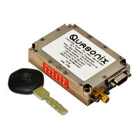
Quasonix TIMTER QSX-V Series Installation And Operation Manual (112 pages)
Multi-mode Digital Telemetry Transmitter
Brand:
Quasonix
| Category:
Transmitter
| Size: 5 MB
Table of Contents
Table of Contents
2
Introduction
9
Description
9
Nomenclature
9
Figure 1: Quasonix Part Number Construction Description
9
Table 1: Model Configuration Example
11
Part Number Field Codes
12
Frequency Bands
12
Table 2: Frequency Band Codes
12
Clock and Data Interface
14
Table 3: Clock and Data Interface Codes
14
Serial Control Interface
15
Table 4: Serial Control Interface Codes
15
ARTM Tier 0 (PCM/FM)
16
ARTM Tier I (SOQPSK-TG)
16
ARTM Tier II (Multi-H CPM)
16
Legacy
16
Table 5: ARTM Tier 0 Codes
16
Table 6: ARTM Tier I Codes
16
Table 7: ARTM Tier II Codes
16
Table 8: Legacy Codes
16
RF Output Power
17
Packages
17
Table 9: RF Output Power Codes
17
Table 10: Package Codes
17
Automatic Carrier Wave Output Option - AC
18
Auto Carrier Save Option - ACS
18
Auxiliary Input Option - AI
18
Figure 2: FPCM Signal on Oscilloscope
18
Adapter Plate - AP
19
Baud Rate Option - Brx
19
CP07 Control Protocol Option - C7
19
Convolutional Encoder Option - CE
19
Clock-Free Baseband Interface Option - CF
20
Figure 3: CCSDS 131.0-B-1 Rendering of Basic Convolutional Encoder Diagram
20
Clock Generator Output Option - CG
21
Dual Power Option - DP
21
Digital Switch Box Option - DSWBX
21
Ethernet Payload Capability - en
21
Table 11: Standard Data Bit Rates and Rate Adaptation Compared to Clock Free Data Bit Rates
21
Analog Frequency Modulation - FM
22
Table 12: Standard Bit Rates Compared to Low/High Rate Options
23
Wide Input Voltage Range Option - WV
26
External Device Control - XD
26
Accessories
27
Fan-Cooled Heat Sink
27
Figure 4: Fan-Cooled Heat Sink and Power Supply
27
Figure 5: Fan-Cooled Heat Sink with 6 Cubic Inch TIMTER
27
Transmitter-Powered Heat Sink (for Airborne Applications)
28
Figure 6: Transmitter-Powered Heat Sink, Pigtail Cable, SMA Extender, and Adapter Plate
28
Figure 7: Transmitter-Powered Heat Sink Mounted on an 04AB Package
29
Figure 8: Transmitter-Powered Heat Sink Mounted on a 07AE Package
29
Adapter Plate
30
Pre-Wired MDM-15 for RS-422 Units
30
Figure 9: Close-Up Using Female MDM-15 Connector
30
Figure 10: Close-Up Using Male MDM-15 Connector
30
Figure 11: Adapter Plate
30
Pre-Wired MDM-15 for TTL Units
31
Wiring Harness for RS-422 Units
31
Figure 12: Pre-Wired MDM-15 with 36" Pigtails for RS-422
31
Figure 13: Pre-Wired MDM-15 with 36" Pigtails for TTL
31
Wiring Harness for TTL Units
32
Ruggedized Handheld Programmer
32
Figure 14: MDM-15 Cable Harness for RS-422
32
Figure 15: MDM-15 Cable Harness for TTL
32
USB to Serial Converter Cable
33
Figure 16: Ruggedized Handheld Programmer
33
Figure 17: USB to Serial Converter Cable
33
Nd Generation Digital Switch Box
34
Figure 18: Digital Switch Box with 18" MDM-9 to MDM-9 Cable Harness
34
Installation Instructions
35
Mechanical
35
Figure 19: 4.2 In3 TIMTER
35
Figure 20: Outline Drawing, TIMTER™ 04AB Telemetry Transmitter
36
Thermal
37
Electrical
37
Figure 21: Example Quasonix Pinout Drawing
38
Figure 22: Baseband Signal Timing
39
Operating Instructions
40
Power-On Operation
40
Dual Power Via Hardware Control
40
2Nd Generation Switch Box Notes
40
TIMTER™ Serial Control Protocol
40
Command Set: Standard and Optional Commands
41
Figure 23: TIMTER™ Welcome Message
41
Table 13: Standard and Optional User Commands
42
Additional Command Set Details
67
Automatic Carrier Output - AC
67
Baseband Clock - BBCK
67
Clock Free Bit Rate - BR
68
Baseband Interface Type - BT
70
Convolutional Encoder - CC
70
Clock Generator Source Select Command - CG
70
Frequency Offset - FO
70
Frequency - FR
71
Internal Clock Rate - IC
71
Input Source Selection Command - IS
71
Low Density Parity Check (LDPC) Command - LD
74
Overtemperature Control - OC
75
RF Output - RF
75
RF Output State - RFS
76
Set Configuration Priority - SC
76
Frequency Sweep - SW
77
System Status Command - SY
77
External Device Control Command - XDC
79
External Device Channel Command - XDCH
80
External Device Frequency Switching Threshold Command - XDF
80
External Device Polarity Invert Command - XDP
81
RF Output Notes
82
Troubleshooting the RF on a Quasonix Transmitter
82
Performance Specifications
85
RF Output
85
Electrical Current
85
Table 14: DC Input Current at Standard Input Voltage
85
Environmental Specifications
86
EMI Performance
86
Table 15: TIMTER™ Environmental Specifications
86
Table 16: TIMTER™ EMI Compliance
86
Carrier Frequency Tuning
87
Table 17: Carrier Frequencies (Mhz)
87
Carrier Frequency Error
89
Bit Error Rate
89
Table 18: Transmitter BER Specifications with Quasonix Demodulator
89
Modulated RF Power Spectrum
90
Table 19: K and M Values Per Waveform
90
Figure 24: PCM/FM (Tier 0) Power Spectral Density with Mask
91
Figure 25: SOQPSK-TG (Tier I) Power Spectral Density with Mask
91
Phase Noise Power Spectrum
92
Figure 26: MULTI-H CPM (Tier II) Power Spectral Density with Mask
92
Baseplate Temperature
93
Vibration and Shock
93
Figure 27: Phase Noise Limit Curve
93
Figure 28: Vibration / Shock Testing System
94
Figure 29: TIMTER™ Mounted for Z-Axis Testing
94
Vibration Testing
95
Figure 30: TIMTER™ Mounted for X-Axis Testing
95
Figure 31: TIMTER™ Mounted for Y-Axis Testing
95
Figure 32: TIMTER™ Vibration Profile
95
Figure 33: Z-Axis Vibration Spectrum
96
Table 20: Random Vibration Spectrum
96
Figure 34: Y-Axis Vibration Spectrum
97
Figure 35: X-Axis Vibration Spectrum
97
Shock Testing
98
Figure 36: Shock Pulse, Z-Axis Positive
98
Figure 37: Shock Pulse, Z-Axis Negative
99
Figure 38: Shock Pulse, Y-Axis Positive
99
Figure 39: Shock Pulse, Y-Axis Negative
100
Figure 40: Shock Pulse, X-Axis Positive
100
Figure 41: Shock Pulse, X-Axis Negative
101
Maintenance Instructions
102
Product Warranty
103
Quasonix Limited Warranty Statement
103
Extended Warranties
104
Technical Support and RMA Requests
105
Appendix A - Preset Option
106
Appendix B - Legacy Binary Protocol Notes
107
Known Limitations of Binary Protocol < V1.005
107
Items Not Supported by the Legacy Transmitter
107
Appendix C - Understanding Clock/Data, AC, and BR
108
Table 21: Transmitter Priority of CS, CF, BR, and AC When RF Is on
108
Figure 42: Transmitter Clock and Data Logic
109
Appendix D - Acronym List
110
Advertisement
Advertisement
Related Products
Quasonix TIMTER
Quasonix nanoTX
Quasonix Categories
Receiver
Transmitter
Data Loggers
Controller
Recording Equipment
More Quasonix Manuals
Login
Sign In
OR
Sign in with Facebook
Sign in with Google
Upload manual
Upload from disk
Upload from URL