Table of Contents
Advertisement
UM1932
User manual
Discovery kit with STM32F469NI MCU
Introduction
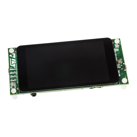
The STM32F469I-DISCO Discovery kit (32F469IDISCOVERY) is a complete demonstration
®
®
and development platform for STMicroelectronics Arm
Cortex
-M4 core-based
2
STM32F469NIH6 microcontroller. This microcontroller features three I
C interfaces, six
2
SPIs with two multiplexed full-duplex I
S interfaces, SDIO, four USART ports, four UART
ports, two CAN buses, three 12-bit ADCs, two 12-bit DACs, one SAI, 8 to 14-bit digital
camera digital module interface, internal 320+4 Kbytes of SRAM and 2-Mbyte Flash
SM
memory, USB HS OTG and USB FS OTG, Ethernet MAC, FMC interface, MIPI DSI
interface, Quad-SPI interface, JTAG debugging support. This Discovery kit offers everything
required for users to get started quickly and develop applications easily.
The hardware features on the board help users to evaluate the following peripherals: USB
OTG FS, microSD™ card, Audio DAC with headset jack, digital microphones, SDRAM,
SM
Quad-SPI Flash memory, 4" TFT LCD using MIPI DSI
interface with capacitive touch
®
panel. The ARDUINO
compatible connectors expand the functionality with a wide choice of
specialized shields. The extension header makes it possible to easily connect a
daughterboard for specific application. The integrated ST-LINK/V2-1 provides an embedded
in-circuit debugger and programmer for the STM32 MCU.
Figure 1. STM32F469I-DISCO board (top view)
Figure 2. STM32F469I-DISCO board (bottom view)
Pictures are not contractual.
April 2020
UM1932 Rev 3
1/30
www.st.com
1
Advertisement
Table of Contents

Related Manuals for STMicroelectronics STM32F469I-DISCO


Summary of Contents for STMicroelectronics STM32F469I-DISCO
-
Page 1: Figure 1. Stm32F469I-Disco Board (Top View)
UM1932 User manual Discovery kit with STM32F469NI MCU Introduction The STM32F469I-DISCO Discovery kit (32F469IDISCOVERY) is a complete demonstration ® ® and development platform for STMicroelectronics Arm Cortex -M4 core-based STM32F469NIH6 microcontroller. This microcontroller features three I C interfaces, six SPIs with two multiplexed full-duplex I... -
Page 2: Table Of Contents
Contents UM1932 Contents Features ........... 6 Ordering information . - Page 3 UM1932 Contents 4.13 Extension connector CN12 ........19 4.14 DSI LCD .
- Page 4 List of tables UM1932 List of tables Table 1. List of available products ........... 7 Table 2.
- Page 5 STM32F469I-DISCO board (bottom view) ........
-
Page 6: Features
Features UM1932 Features • STM32F469NIH6 microcontroller with 2 Mbytes of Flash memory and 324 Kbytes of RAM, in BGA216 package • 4-inch 800x480 pixel TFT color LCD with MIPI DSI interface and capacitive touch screen • USB OTG FS • SAI audio DAC •... -
Page 7: Ordering Information
Codification The meaning of the codification is explained in Table Table 2. Codification explanation STM32F4XXY-DISCO Description Example: STM32F469I-DISCO MCU series in STM32 32-bit Arm Cortex STM32F4 STM32F4 Series MCUs MCU product line in the series STM32F469... -
Page 8: Development Environment
USB Type-A to Mini-B cable Development toolchains • IAR™ - EWARM • Keil® - MDK-ARM • STMicroelectronics - STM32CubeIDE ® • Mbed™ online (see mbed.org) Demonstration software The demonstration software, included in the STM32Cube MCU Package corresponding to the on-board microcontroller, is preloaded in the STM32 Flash memory and in the external on-board Flash memory for easy demonstration of the device peripherals in standalone mode. -
Page 9: Hardware Layout And Configuration
UM1932 Hardware layout and configuration Hardware layout and configuration The STM32F469I-DISCO Discovery board is designed around the STM32F469NIH6 (216- pin TFBGA package). Figure 3 illustrates the connection between the STM32F469NIH6 and the peripherals (SDRAM, Quad-SPI Flash memory, color LCD, USB OTG connector, Audio, C extension connector, microSD™... -
Page 10: Figure 4. Stm32F469I-Disco Top Side Layout
Hardware layout and configuration UM1932 Figure 4. STM32F469I-DISCO top side layout LD1, LD2, LD3, LD4: Digital green, orange, red, blue microphone LEDs respectively SB17 Solder bridge 4-inch DSI LCD VBUS LED VBUS LED SB18 Solder bridge Digital Digital microphone microphone... -
Page 11: Figure 5. Stm32F469I-Disco Bottom Side Layout
UM1932 Hardware layout and configuration Figure 5. STM32F469I-DISCO bottom side layout Power selection ST-LINK/V2-1 jumper 5 V LED Reset button ST-LINK/V2-1 Wake-up COM LED button Audio jack CN5, CN6, CN7, CN8 ® ARDUINO connectors microSD™ card STM32F469NIH6 CN11 C extension... -
Page 12: Embedded St-Link/V2-1
10 PC via USB, a driver for ST-LINK/V2-1 must be installed. It can be downloaded from the www.st.com webpage. If the STM32F469I-DISCO board is connected to the PC before installing the driver, the ® Windows device manager may report some USB devices found on STM32F469I-DISCO as “Unknown”. -
Page 13: Power Supply
4.2.2 Supplying the board through ST-LINK/V2-1 USB port To power the STM32F469I-DISCO board in this way, the USB host (a PC) gets connected with the STM32F469I-DISCO board via a USB cable to the ST-LINK/V2-1 connector. In the first step, only the ST-LINK part U3 is powered by the PC. In fact, before USB enumeration, the host PC provides only 100 mA to the board at that time. -
Page 14: Measurement Of Current Idd Drawn By The Stm32F469Ni
The ST890 power switch protects the USB port of the host against current demand exceeding 600 mA, should a short-circuit occur on the board. The STM32F469I-DISCO board can also be supplied from a USB power source not supporting enumeration, such as a USB charger. In this particular case, the solder bridge SB16 must be closed. -
Page 15: Clock Source
The 32.768 kHz crystal X3 is the clock source for the embedded RTC. Reset source The reset signal of STM32F469I-DISCO board is low active and the reset sources include: • Reset button B1, providing solder bridge SB1 is closed (default setting) •... -
Page 16: Audio Outputs
An USB OTG full speed communication is available at connector CN13. The STM32F469I-DISCO Discovery board can be powered by the 5 V DC of this USB OTG FS connection. When the STM32F469I-DISCO is USB host, it supplies the USB peripheral. -
Page 17: Microsd™ Card
CN5, CN6, CN7 and CN8 are female connectors compatible with the ARDUINO standard. ® Most shields designed for ARDUINO Uno V3 can fit to the STM32F469I-DISCO Discovery board. ® Caution: The STM32 microcontroller I/Os are 3.3 V compatible while ARDUINO Uno boards are 5 V compatible. -
Page 18: Table 5. Arduino ® Compatible Connectors
1. Before using pin4 of CN6 as +3.3V input, the solder bridge SB8 must be removed. Otherwise the board STM32F469I-DISCO could be damaged by the over-current. 2. The external voltage applied to pin VIN must be in the range from 6 V to 9 V at 25°C ambient temperature. -
Page 19: Extension Connector Cn12
The extension connector CN12 is a 2.54 mm pitch header located at the bottom side of the STM32F469I-DISCO Discovery board. It is composed of 16 square pins of 0.64 mm arranged in double row and it is compatible with usual connectors mating with 2.54 mm headers, having 0.64 mm square posts. - Page 20 Table 6. Extension connector pinout Extension connector MCU Port NRST PB13 PA15 PB12 PC13 CAN2 USART6 I2S2 SPI1 MOSI TIM3/TI TIM3/ TIM2_ TIM1_ TIM3_ TIM1_ TIM1_ TIMER MISO TIM8_ CH1/2 CH1N BKIN _ETR ADC1/AD ADC123 C2_IN5 _IN11 ANTI Speaker Speaker SYSTEM +3V3 MCO1 NRST...
-
Page 21: Dsi Lcd
R117 is soldered, R119 is not soldered. • The STM32F469I-DISCO Discovery board offers the option to control the EN pin by HW through port PA3. In such case, R117 must be removed and R119 soldered. -
Page 22: Buttons And Leds
The black button B1 located bottom side is the reset of the microcontroller STM32F469NIH6. Refer to the Figure 5: STM32F469I-DISCO bottom side layout The blue button B2 located bottom side is available to be used as a digital input or as alternate function Wake-up. -
Page 23: C Extension Connector Cn11
UM1932 Hardware layout and configuration 4.16 C extension connector CN11 Figure 8. I C extension connector (front view) MS30715V2 Table 9. I C extension connector pinout Pin number Description Pin number Description I2C1_SDA (PB9) +3V3 I2C1_SCL (PB8) EXT_RESET(PB0) 4.17 USB OTG FS Micro-AB connector CN13 Figure 9. -
Page 24: Microsd™ Connector Cn9
Hardware layout and configuration UM1932 4.18 microSD™ connector CN9 Figure 10. microSD™ connector CN9 (front view) Table 11. microSD™ connector CN9 Description Description number number SDIO_D2 (PC10) SDIO_D3 (PC11) SDIO_D0 (PC8) SDIO_CMD (PD2) SDIO_D1 (PC9) +3.3V SDIO_CLK (PC12) MicroSDcard_detect (PG2) 24/30 UM1932 Rev 3... -
Page 25: St-Link/V2-1 Usb Mini-B Connector Cn1
Table 12. USB Mini-B connector CN1 Pin number Description Pin number Description VBUS (power) Shield 4.20 Audio jack CN3 A 3.5 mm stereo audio jack CN3 is available on STM32F469I-DISCO discovery board to connect a headphone. UM1932 Rev 3 25/30... -
Page 26: Appendix A Mechanical Dimensions
Mechanical dimensions UM1932 Appendix A Mechanical dimensions Figure 12. Mechanical dimensions in millimeter 26/30 UM1932 Rev 3... -
Page 27: Appendix B Federal Communications Commission (Fcc)
B.1.2 Part 15.21 Any changes or modifications to this equipment not expressly approved by STMicroelectronics may cause harmful interference and void the user’s authority to operate this equipment. B.1.3 Part 15.105 This equipment has been tested and found to comply with the limits for a Class B digital device, pursuant to part 15 of the FCC Rules. -
Page 28: Appendix Cce Conformity
CE conformity UM1932 Appendix C CE conformity Warning EN 55032 / CISPR32 (2012) Class B product Warning: this device is compliant with Class B of EN55032 / CISPR32. In a residential environment, this equipment may cause radio interference. Avertissement : cet équipement est conforme à la Classe B de la EN55032 / CISPR 32. Dans un environnement résidentiel, cet équipement peut créer des interférences radio. -
Page 29: Revision History
UM1932 Revision history Revision history Table 13. Document revision history Date Version Revision Details 19-Sep-2015 Initial release. Updated Figure 3: Hardware block diagram Added Section Appendix B: Federal Communications 20-Oct-2015 Commission (FCC) and Industry Canada (IC) Compliance Section 2: Ordering information. Removed Technology partners and Schematics. - Page 30 IMPORTANT NOTICE – PLEASE READ CAREFULLY STMicroelectronics NV and its subsidiaries (“ST”) reserve the right to make changes, corrections, enhancements, modifications, and improvements to ST products and/or to this document at any time without notice. Purchasers should obtain the latest relevant information on ST products before placing orders.
Need help?
Do you have a question about the STM32F469I-DISCO and is the answer not in the manual?
Questions and answers