Table of Contents
Advertisement
Quick Links
Advertisement
Table of Contents

Related Manuals for Terasic TR4


Summary of Contents for Terasic TR4
- Page 1 TR4 User Manual www.terasic.com March 30, 2017...
-
Page 2: Table Of Contents
EATURES 1.3 B ..............................3 OARD VERVIEW 1.4 B ..............................4 LOCK IAGRAM 1.5 A ................................. 8 SSEMBLY USING THE TR4 BOARD CHAPTER 2 ........................ 9 2.1 C ............................9 ONFIGURATION PTIONS 2.2 S ..............................16 ETUP LEMENTS 2.3 S .............................. - Page 3 3.9 I ................................. 69 NFORMATION TR4 SYSTEM BUILDER CHAPTER 4 ........................ 71 4.1 I ............................... 71 NTRODUCTION 4.2 G ............................72 ENERAL ESIGN 4.3 U TR4 S ..........................73 SING YSTEM UILDER EXAMPLES OF ADVANCED DEMONSTRATION CHAPTER 5 ..............83 5.1 B...
-
Page 4: Chapter 1 Overview
The advantages of the Stratix® IV GX FPGA platform with integrated transceivers have allowed the TR4 to be fully compliant with version 2.0 of the PCI Express standard. This will accelerate mainstream development of PCI Express-based applications and enable customers to deploy designs for a broad range of high-speed connectivity applications. -
Page 5: Key Features
Three on-board programmable PLL timing chips SMA connector pair for differential clock input SMA connector pair for differential clock output SMA connector for external clock input SMA connector for clock output TR4 User Manual www.terasic.com March 30, 2017... -
Page 6: Board Overview
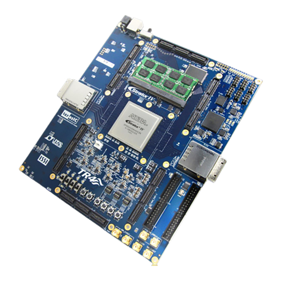
Figure 1-1 Figure 1-2 show the top and bottom view of the TR4 board. It depicts the layout of the board and indicates the location of the connectors and key components. Users can refer to these figures for relative location when the connectors and key components are introduced in the following chapters. -
Page 7: Block Diagram
Figure 1-2 TR4 Board View (Bottom) Figure 1-3 shows the block diagram of the TR4 board. To provide maximum flexibility for the users, all key components are connected with the Stratix IV GX FPGA device, allowing the users to implement any system design. - Page 8 Figure 1-3 TR4 Block Diagram Below is more detailed information regarding the blocks in Figure 1-3. Stratix IV GX FPGA EP4SGX230C2 228,000 logic elements (LEs) 17,133 total memory Kb 1,288 18x18-bit multipliers blocks 2 PCI Express hard IP blocks TR4 User Manual www.terasic.com...
- Page 9 2MB SSRAM (512K x 32) DDR3 SO-DIMM Socket Up to 4GB capacity Maximum memory clock rate at 533MHz Theoretical bandwidth up to 68Gbps LEDs 4 user-controllable LEDs Active-low| TR4 User Manual www.terasic.com March 30, 2017...
- Page 10 Among HSMC Port A to D, there are 55 true LVDS TX channels to 1.6Gbps and 17 emulated LVDS TX channels up to 1.1Gbps whereas there are 9 additional TX channels from HSMC Port E. Configurable I/O standards - 1.5V, 1.8V, 2.5V, 3.0V Two 40-pin GPIO Expansion Headers TR4 User Manual www.terasic.com March 30, 2017...
-
Page 11: Assembly
Temperature Sensor Cooling Fan Attach the included rubber (silicon) foot stands, as shown in Figure 1-4, to each of the four copper stands on the TR4 board. Figure 1-4 Mount Silicon Foot Stands TR4 User Manual www.terasic.com March 30, 2017... -
Page 12: Using The Tr4 Board
Programming through Flash JTAG FPGA Programming with USB-Blaster The USB-blaster is implemented on the TR4 board to provide a JTAG configuration through the on-board USB-to-JTAG configuration logic through the type-B USB connector, an FTDI USB 2.0 PHY device, and an Altera MAX II CPLD. For this programming mode, configuration data will be lost when the power is turned off. -
Page 13: Flash Programming
Make sure that power is provided to the TR4 board. Open JP7 to bypass the JTAG interface of the HSMC if it won’t be used. Connect the USB cable supplied directly to the USB Blaster port of the TR4 board (see Figure 2-1). -
Page 14: Software Requirements
Nios II IDE 11.1 or later Program_Flash folder contents: Program_Flash.bat Program_Flash.pl Program_Flash.sh tr4_default_flash_loader.sof boot_loader_cfi.srec Before you use the program_Flash.bat batch file to program the flash memory, make sure the TR4 is TR4 User Manual www.terasic.com March 30, 2017... - Page 15 .elf file you wish to program/convert in the Program_Flash directory. Programming Flash Memory with .sof using Program_Flash.bat 1. Launch the program_Flash.bat batch file from the directory (\demonstrations\TR4_<Stratix device>\ TR4_Default_Flash_Loaderr\Program_Flash) of the TR4 system CD-ROM. 2. The Flash program tool shows the menu options. Figure 2-3 Flash Program Tools 3.
- Page 16 Figure 2-4 Option 2 4. Enter the .sof file name to be programmed onto the flash memory. Figure 2-5 Enter .sof Name to Program TR4 User Manual www.terasic.com March 30, 2017...
- Page 17 Please make sure Quartus II 11.1 and Nios II 11.1 IDE or later is used. Figure 2-6 Loading .sof File Erasing Flash. TR4 User Manual www.terasic.com March 30, 2017...
- Page 18 Figure 2-7 Erasing Flash Programming Flash. Figure 2-8 Programming Flash Programming complete. TR4 User Manual www.terasic.com March 30, 2017...
-
Page 19: Setup Elements
Figure 2-9 Programming Flash complete JTAG Control DIP Switch The TR4 supports individual JTAG interfaces on each HSMC connector. This feature allows users to extend the JTAG chain to daughter cards or additional TR4s. Before using this interface, JP7 needs to be shorted to enable the JTAG interface on all the HSMC connectors. -
Page 20: Status Elements
ON: HSME TOP in-chain OFF: Bypass HSME TOP position 2 HSMCF_TOP ON: HSMF TOP in-chain OFF: Bypass HSMF TOP The TR4 includes status LEDs. Please refer Table 2-2 for the status of the LED indicator. Table 2-2 LED Indicators Board... -
Page 21: General User Input /Output
D1~D12 HSMC VCCIO_LED Table 2-12) Push-buttons The TR4 includes six push-buttons that allow you to interact with the Stratix IV GX FPGA. Each of these buttons is debounced using a Schmitt Trigger circuit, as indicated in Figure 2-10. Each... - Page 22 PIN_D12 Slide Switches There are four slide switches on the TR4 to provide additional FPGA input control. Each switch is connected directly to a pin of the Stratix IV GX FPGA. When a slide switch is in the DOWN...
-
Page 23: High -Speed Mezzanine Cards
HSMC C, HSMC D, HSMC E, and HSMC F. Each group has a male and female HSMC port on the top and bottom side of the TR4 board except HSMC E and HSMC F. In addition, both the male and female HSMC connector share the same I/O pins besides JTAG interface and high-speed serial I/O (transceivers). -
Page 24: Lvds Interface
Due to the limitation of FPGA bank I/O distribution and dedicated clock in/out pin numbers, there are some differences between individual HSMC connectors, listed below: LVDS Interface On the TR4 board, only HSMC ports A, B, C and D support LVDS. Each HSMC port provides 18(1) LVDS channel transceivers. - Page 25 (1) Although the specifications of the HSMC connector defines signals D0~D3 as single-ended I/Os, D0 and D2 can be used as LVDS transmitters and D1 and D3 can be used as LVDS receivers on the TR4. Figure 2-12 Emulated LVDS Resistor Network between FPGA and HSMC Port TR4 User Manual www.terasic.com...
- Page 26 Reference name of the differential termination resistor HSMB_RX_p[11] R333 HSMB_RX_p[12] R318 HSMB_RX_p[13] R312 HSMB_RX_p[14] R311 HSMB_RX_p[15] R303 HSMB_RX_p[16] R315 HSMB_D[1] R332 HSMC_RX_p[0] R314 HSMC_RX_p[1] R316 HSMC_RX_p[2] R330 HSMC_RX_p[3] R341 HSMC_RX_p[4] R329 HSMC_RX_p[5] R328 HSMC_RX_p[6] R309 TR4 User Manual www.terasic.com March 30, 2017...
-
Page 27: I2C Interface
The I2C bus on the HSMC connectors is separated into two groups. HSMC Port A, B, and C share the same I2C interface. HSMC ports D, E, and F share the other I2C bus. Table 2-10 lists the detailed distribution. Table 2-10 HSMC I2C Group TR4 User Manual www.terasic.com March 30, 2017... -
Page 28: Power Supply
HSMD_SDA data signal (1) The I2C I/O on the TR4 HSMC connector is defined with 3.3V. There is a level translator between FPGA and HSMC connector to translate FPGA 2.5V or 1.5V I/O to 3.3V. The signals above are also connected to the level translator. When these signals are used as general purpose I/O, the maximum data rate is 60Mbps. - Page 29 Users who don’t need the power from the HSMC can remove these fuses to cut the power on connector. CAUTION. Before powering on the TR4 board with a daughter card, please check to see if there is a short circuit between the power pins and FPGA I/O.
- Page 30 I/O standard between TR4 HSMC connector pins and daughter card system. For example, if the I/O standard of HSMC pins on TR4 board is set to 1.8V, a daughter card with 3.3V or 2.5V I/O standard may not work properly on TR4 board due to I/O standard mismatch. When using custom or third-party HSMC daughter cards, make sure that all the pin locations are aligned to prevent shorts.
- Page 31 SW4 and SW6. SW5 is used to control the HSMC JTAG chain on the bottom-side of the TR4. Only when multiple TR4s are stacked should the boards use this switch. A document titled Using_Multi-TR4_system.pdf in the TR4 system CD will give an example to demonstrate how to set SW5 to connect JTAG chains together for multiple TR4 boards.
- Page 32 Figure 2-16. Figure 2-16 JTAG Chain for a Standalone TR4 If the HSMC-based daughter card connected to the HSMC connector uses the JTAG interface, the 4-position DIP switch (SW4 or SW6) should be set to ‘On’ according to the HSMC port used. In HSMC Port D is used so position 4 of the SW4 switch is set to ‘On’.
- Page 33 Figure 2-17 JTAG Chain for a Daughter Card (JTAG is used) Connected to HSMC Port D of the TR4 Figure 2-18 JTAG chain for a Daughter Card (JTAG not used) Connected to HSMC Port D of the TR4 TR4 User Manual www.terasic.com...
- Page 34 Multi-FPGA High-Capacity Platforms through HSMC The TR4 offers a selection of two Stratix IV GX devices, EP4SGX230 and EPSGX530, which offer logic elements (LEs) up to 228,000 and 531,200, respectively, to provide the flexibility for users to select a suitable device. In situations where users’ design exceeds the capacity of the FPGA, the HSMC interface can be used to connect to other FPGA system boards creating a multi-FPGA scalable system.
-
Page 35: Gpio Expansion Headers
Figure 2-20 Two TR4 Boards Connected via HSMC Cable The TR4 consists of two 40-pin expansion headers as shown in Figure 2-21. Each header has 36 I/O pins connected to the Stratix IV GX FPGA, with the other 4 pins providing 5V (VCC5) DC, 3.3V (VCC33) DC, and two GND pins. - Page 36 Figure 2-21 Pin Distribution of the GPIO Expansion Headers Finally, Figure 2-22 shows the connections between the GPIO expansion headers and Stratix IV TR4 User Manual www.terasic.com March 30, 2017...
- Page 37 GPIO Expansion 0 IO[12] PIN_AK34 GPIO0_D13 GPIO Expansion 0 IO[13] PIN_AL34 GPIO0_D14 GPIO Expansion 0 IO[14] PIN_AK35 GPIO0_D15 GPIO Expansion 0 IO[15] PIN_AL35 GPIO0_D16 GPIO Expansion 0 IO[16] PIN_AM34 GPIO0_D17 GPIO Expansion 0 IO[17] PIN_AN34 TR4 User Manual www.terasic.com March 30, 2017...
- Page 38 GPIO Expansion 1 IO[14] PIN_AV31 GPIO1_D15 GPIO Expansion 1 IO[15] PIN_AG24 GPIO1_D16 GPIO Expansion 1 IO[16] PIN_AL27 GPIO1_D17 GPIO Expansion 1 IO[17] PIN_AW27 GPIO1_D18 GPIO Expansion 1 IO[18] PIN_AH26 GPIO1_D19 GPIO Expansion 1 IO[19] PIN_AW28 TR4 User Manual www.terasic.com March 30, 2017...
-
Page 39: Ddr3 So-Dimm
DDR3 ADDRess [4] SSTL-15 Class I PIN_P24 mem_addr [5] DDR3 ADDRess [5] SSTL-15 Class I PIN_A24 mem_addr [6] DDR3 ADDRess [6] SSTL-15 Class I PIN_M21 mem_addr [7] DDR3 ADDRess [7] SSTL-15 Class I PIN_D17 TR4 User Manual www.terasic.com March 30, 2017... - Page 40 PIN_F15 mem_dq[2] DDR3 Data [2] SSTL-15 Class I PIN_C16 mem_dq[3] DDR3 Data [3] SSTL-15 Class I PIN_B16 mem_dq[4] DDR3 Data [4] SSTL-15 Class I PIN_G17 mem_dq[5] DDR3 Data [5] SSTL-15 Class I PIN_A16 TR4 User Manual www.terasic.com March 30, 2017...
- Page 41 PIN_E28 mem_dq[37] DDR3 Data [37] SSTL-15 Class I PIN_D28 mem_dq[38] DDR3 Data [38] SSTL-15 Class I PIN_H26 mem_dq[39] DDR3 Data [39] SSTL-15 Class I PIN_J26 mem_dq[40] DDR3 Data [40] SSTL-15 Class I PIN_F19 TR4 User Manual www.terasic.com March 30, 2017...
- Page 42 DDR3 Data Strobe n[1] Differential 1.5-V SSTL Class I PIN_J16 mem_dqs_n[2] DDR3 Data Strobe n[2] Differential 1.5-V SSTL Class I PIN_K23 mem_dqs_n[3] DDR3 Data Strobe n[3] Differential 1.5-V SSTL Class I PIN_B28 TR4 User Manual www.terasic.com March 30, 2017...
-
Page 43: Clock Circuitry
Figure 2-23 Connection between DDR3 and Stratix IV GX FPGA Stratix IV GX FPGA Clock Inputs and Outputs The TR4 development board contains three types of clock inputs which include 26 global clock input pins, external PLL clock inputs and transceiver reference clock inputs. The clock input TR4 User Manual www.terasic.com... - Page 44 Stratix IV GX FPGA originate from on-board oscillators, a 50MHz, driven through the clock buffers as well as other interfaces including HSMC, GPIO expansion headers(share pins with HSMC Port C), and SMA connectors. The overall clock distribution of the TR4 is presented in Figure 2-24.
- Page 45 Figure 2-24 Clock Connections of the TR4 TR4 User Manual www.terasic.com March 30, 2017...
- Page 46 PCI Express (PIPE) and the SMA connectors. The TR4 uses three programmable low-jitter clock generators with default clock output of 100MHz and an I/O standard of LVDS that is non-configurable. The clock generators are programmed via Max II CPLD to generate the necessary clocks for the Stratix IV GX transceiver protocols and interfaces such as HSMC.
- Page 47 PCIe connector. The clock frequency for the programmable clock generators can be specified by using the TR4 control panel, TR4 system builder, or the external clock generator demo provided. The associated pin assignments for clock buffer and SMA connectors to FPGA I/O pins are shown Table 2–20.
-
Page 48: Pci Express
2-26) will be used to connect TR4 board and PCIe add-in card as shown Figure 2-27, the longest length up to 3 meters. These two associated devices are not included in TR4 kit. To purchase the PCA card as well as the external cable, please refrence Terasic website pca.terasic.com and PCIe_Cable.terasic.com. - Page 49 Figure 2-25 PCIe Cabling Adaptor(PCA) card Figure 2-26 PCIe External Cable TR4 User Manual www.terasic.com March 30, 2017...
- Page 50 Figure 2-27 PCIe Link Setup between TR4 and PC Figure 2-28 PCI Express Pin Connection TR4 User Manual www.terasic.com March 30, 2017...
-
Page 51: Flash Memory
PCIE1_TX_p[3] 1.4-V PCML PCIE1_RX_p[3] input The TR4 development board features a 64MB Intel CFI-compliant NOR-type flash memory device which is part of the shared FMS Bus consisting of flash memory, SSRAM, and the Max II CPLD TR4 User Manual www.terasic.com... - Page 52 CPLD (EPM2210) can access flash for FPP configuration of the FPGA using the PFL Megafunction. Table 2-18 lists the flash pin assignments, signal names, and functions. Figure 2-29 Connection between Flash, SSRAM, MAXII EPM2210 and the Stratix IV GX FPGA TR4 User Manual www.terasic.com March 30, 2017...
- Page 53 3.0-V PCI-X PIN_N29 FSM_D10 Data bus 3.0-V PCI-X PIN_P29 FSM_D11 Data bus 3.0-V PCI-X PIN_T27 FSM_D12 Data bus 3.0-V PCI-X PIN_AM17 FSM_D13 Data bus 3.0-V PCI-X PIN_AL17 FSM_D14 Data bus 3.0-V PCI-X PIN_AK16 TR4 User Manual www.terasic.com March 30, 2017...
-
Page 54: Ssram Memory
1.5 V PIN_A20 The Synchronous Static Random Access Memory (SSRAM) device featured on the TR4 development board is part of the shared Flash-SSRAM-Max II (FSM) bus, which connects to Flash memory, SSRAM, and the MAX II CPLD (EEPM2210) System Controller. This device is a 2MB synchronously pipelined and high-speed, low-power synchronous static RAM designed to provide burstable, high-performance memory for communication and networking applications. - Page 55 3.0-V PCI-X PIN_AN16 SSRAM_BE_n1 Synchronous Byte Write Controls 3.0-V PCI-X PIN_AN17 SSRAM_BE_n2 Synchronous Byte Write Controls 3.0-V PCI-X PIN_AR16 SSRAM_BE_n3 Synchronous Byte Write Controls 3.0-V PCI-X PIN_AU16 SSRAM_CE1_n Synchronous Chip Enable 3.0-V PCI-X PIN_AF17 TR4 User Manual www.terasic.com March 30, 2017...
-
Page 56: Temperature Sensor And Fan
Stratix IV GX FPGA. The 7-bit power-on-reset (POR) slave address for this sensor is ‘0011000b’. An optional 3-pin +12V header for fan control located on J10 of the TR4 board is intended to reduce the temperature of the FPGA. When the temperature of the FPGA device is over the threshold value set by the users, the fan will turn on automatically. -
Page 57: Ecurity
ON position, the board is powered on. Alternatively when the switch is in the OFF position, the board is powered off. The TR4 board features design security to protect your designs against unauthorized copying, reverse engineering, and tampering of your configuration files. For more information, please refer to Altera’s application note, “AN556: Using the Design Security Features in Altera FPGAs”... - Page 58 Figure 2-31 R199~R201 Position on TR4 TR4 User Manual www.terasic.com March 30, 2017...
-
Page 59: Chapter 3 Control Panel
The Control Panel software utility is located in the directory “/Tools/TR4_ControlPanel” in the TR4 System CD. To execute the program, simply copy the whole folder to your host computer and launch the control panel by double clicking the TR4_ControlPanel.exe. - Page 60 The Control Panel will occupy the USB port; users will not be able to download any configuration file into the FPGA before you exit the Control Panel program. Figure 3-1 Download .sof Files to the TR4 board The Control Panel is now ready, as shown in Figure 3-2.
- Page 61 Figure 3-2 TR4 Control Panel is Ready If the connection between TR4 board and USB-Blaster is not established, or the TR4 board is not powered on before running the TR4_ControlPanel.exe, the Control Panel will fail to detect the FPGA and a warning message window will pop up as shown in Figure 3-3.
- Page 62 Figure 3-3 The TR4 Control Panel Fails to Download .sof File 3-4. The “Control Codes” which The concept of the TR4 Control Panel is illustrated in Figure performs the control functions is implemented in the FPGA board. It communicates with the Control Panel window, which is active on the host computer, via the USB Blaster link.
-
Page 63: Controlling The Led S
The TR4 Control Panel can be used to illuminate the LEDs, monitoring buttons/switches status, read/write from various memory types, in addition to testing various components of the TR4 board. One of the functions of the Control Panel is to set up the status of the LEDs. The tab-window shown... -
Page 64: Switches And Push -Buttons
Choose the Button tab as shown in Figure 3-6. This function is designed to monitor status of switches and buttons from a graphical user interface in real-time. It can be used to verify the functionality of switches and buttons. TR4 User Manual www.terasic.com March 30, 2017... -
Page 65: Memory Controller
Figure 3-6 Monitoring Switches and Buttons The Control Panel can be used to write/read data to/from the DDR3 SO-DIMM/Flash/SSRAM memory on the TR4 board. We will describe how the DDR3 SO-DIMM is accessed. Click on the Memory tab to reach the tab-window shown in Figure 3-7. - Page 66 Press Load Memory Content to a File button. When the Control Panel responds with the standard Windows dialog box ask for the destination file, users can specify the desired file in the usual manner. TR4 User Manual www.terasic.com March 30, 2017...
- Page 67 Figure 3-7 Access DDR3 SO-DIMM Memory TR4 User Manual www.terasic.com March 30, 2017...
-
Page 68: Temperature Monitor
Control Panel. The temperatures of Stratix IV GX and TR4 board are shown on the right-hand side of the Control Panel. When the temperature of Stratix IV GX exceeds the maximum setting of ‘Over Temperature’ or ‘Alert’, a warning message will be shown on the Control Panel. -
Page 69: Pll
Figure 3-9 Accessing the Temperature Sensor through Control Panel The PLL function is designed to configure the external programmable PLL on the TR4. There are 3 programmable clocks for the TR4 board that generates reference clocks for the following signals HSMA_REFCLK_p/n, HSMB_REFCLK_p/n, and PGM_GXBCLK_p1/n1. -
Page 70: Hsmc
‘Verify’. Note the Control Panel HSMC loopback test does not test the transceiver signals on the HSMC interface. For HSMC transceiver loopback test, please refer to the demonstration section. CAUTION. Turn off the TR4 board before the HSMC loopback adapter is mounted to prevent any damage to the TR4 board. TR4 User Manual www.terasic.com... -
Page 71: Fan
Choose the Fan tab to reach the window shown in Figure 3-12. This function is designed to verify the functionality of the fan components and signals. Please make sure the fan is installed on the TR4 before running this function. TR4 User Manual www.terasic.com... -
Page 72: Information
Figure 3-12 Fan Control of the TR4 For more information, please click on the Information button in order to reach the window shown in 3-13., Users can click “Terasic Web” button and “TR4_Web” button to reach the respective Figure websites in order to learn more about the TR4 and Terasic Technologies. - Page 73 Figure 3-13 Information Tab of TR4 Control Panel TR4 User Manual www.terasic.com March 30, 2017...
-
Page 74: Tr4 System Builder
Chapter 4 TR4 System Builder This chapter describes how users can create a custom design project on the TR4 board by using the included TR4 software tool – TR4 System Builder. The TR4 System Builder is a Windows-based software utility, designed to assist users in creating a Quartus II project for the TR4 board within minutes. -
Page 75: General Design Flow
This section will introduce the general design flow to build a project for the TR4 board via the TR4 System Builder. The general design flow is illustrated in the Figure 4-1. Users should launch TR4 System Builder and create a new project according to their design requirements. -
Page 76: Using Tr4 System Builder
Figure 4-1 General Design Flow This section provides the detail procedures on how the TR4 System Builder is used. Install and launch the TR4 System Builder The TR4 System Builder is located in the directory: "Tools\TR4_SystemBuilder" in the TR4 System CD. Users can copy the whole folder to a host computer without installing the utility. - Page 77 Select the target board type and input project name as show in Figure 4-3. Board Type: Select the appropriate FPGA device according to the TR4 board which includes the EP4SGX230 and EP4SGX530 devices. Project Name: Specify the project name as it is automatically assigned to the name of the top-level design entity.
- Page 78 If the component is enabled, the TR4 System Builder will automatically generate the associated pin assignments including the pin name, pin location, pin direction, and I/O standards.
- Page 79 PLLs. Note. If users need to dynamically change the frequency, they will need to modify the generated control code themselves. Figure 4-5 External Programmable PLL TR4 User Manual www.terasic.com March 30, 2017...
- Page 80 Users can connect HSMC-interfaced daughter cards onto the HSMC ports located on the TR4 board shown in Figure 4-6. Select the daughter card you wish to add to your design under the appropriate HSMC connector where the daughter card is connected to. The System Builder will automatically generate the associated pin assignment including pin name, pin location, pin direction, and IO standard.
- Page 81 Figure 4-7 Specify Prefix Name for HSMC Expansion Board Additionally, users can choose the “HSMC-C/GPIO” as either “HSMC” or “GPIO”, since the GPIO ports share pins with HSMC Port C as shown in Figure 4-8. TR4 User Manual www.terasic.com March 30, 2017...
- Page 82 After users select the “GPIO” option, a “GPIO Edit” button will appear. If this is clicked, a “GPIO Expansion” window will pop up for users to select a compatible Terasic daughter card. Once a daughter card selected, the JP4 header diagram in the upper left hand corner of the window, which...
- Page 83 Figure 4-9 GPIO option and I/O standard recommend The TR4 System Builder also provides functions to restore a default setting, loading a setting, and saving users’ board configuration file shown in Figure 4-10. Users can save the current board configuration information into a .cfg file and load it to the TR4 System Builder.
- Page 84 Figure 4-10 Project Settings When users press the Generate button, the TR4 System Builder will generate the corresponding Quartus II files and documents as listed in the Table 4-1 in the directory specified by the user. Table 4-1 Files Generated by TR4 System Builder...
- Page 85 // 1T 50MHz .conf_rd(), // 1T 50MHz // status .conf_ready(), // 2-wire interface .max_sclk(MAX2_I2C_SCL), .max_sdat(MAX2_I2C_SDA) If dynamic PLL configuration is required, users need to modify the code according to users’ desired PLL behavior. TR4 User Manual www.terasic.com March 30, 2017...
-
Page 86: Examples Of Advanced Demonstration
This chapter introduces several advanced designs that demonstrate Stratix IV GX features using the TR4 board. The provided designs include the major features on board such as the HSMC connectors, PCIe, and DDR3. For each demonstration the Stratix IV GX FPGA configuration file is provided, as well as full source code in Verilog HDL. -
Page 87: External Clock Generator
FPGA Configuration File: Breathing_LEDs.sof Make sure Quartus II and Nios II are installed on your PC. Connect the USB Blaster cable to the TR4 board and host PC. Install the USB Blaster driver if necessary. Power on the TR4 board. - Page 88 This section describes the operation for the EXT_PLL_CTRL instruction hardware port. Figure 5-2 shows the EXT_PLL_CTRL instruction block diagram connected to the MAX II EPM2210 device. The EXT_PLL_CTRL controller module is defined by a host device, the Stratix IV GX FPGA and a TR4 User Manual www.terasic.com March 30, 2017...
- Page 89 MAX II EPM2210. Through the I2C bus interface, the EXT_PLL_CTRL controller is able to control the Max II device by specifying the desire clock outputs set by the user. By changing the IP parameters of the Terasic EXT_PLL_CTRL IP, the external clock output frequency can be adjusted accordingly.
- Page 90 Write Timing Waveform: As BUTTON0 (the trigger source defined by Terasic) is pressed, the 'conf_wr' signal is on the rising edge, serial data is transferred immediately with the 'conf_ready' signal in the transmission period starting at falling edge level as shown in Figure 5-3.
- Page 91 Figure 5-3 Write Timing Waveform As BUTTON1 (the trigger source defined by Terasic) is pressed the 'conf_rd' signal is on the rising edge, the user settings are read back immediately once the 'conf_ready' signal is on the falling edge 5-4. As the transfer is complete, the ‘conf_ready’ returns back to original state...
- Page 92 Figure 5-4 Read Timing Waveform Quartus II 11.1 Project directory: TR4_EXT_PLL Bit stream used: TR4_EXT_PLL.sof Demonstration Batch File Demo Batch File Folder: TR4_EXT_PLL\demo_batch Batch File: TR4_EXT_PLL.bat FPGA Configuration File: TR4_EXT_PLL.sof TR4 User Manual www.terasic.com March 30, 2017...
-
Page 93: High Speed Mezzanine Card (Hsmc)
Make sure Quartus II is installed on your PC. Connect the USB Blaster cable to the TR4 board and host PC. Install the USB Blaster driver if necessary. Power on the TR4 board. Execute the demo batch file “TR4_EXT_PLL.bat” under the batch file folder, TR4_EXT_PLL\demo_batch ... - Page 94 Check that Quartus II and Nios II are installed on your PC. Insert the HSMC loopback daughter card onto the HSMC Port E as shown in Figure 5-5. Connect the USB Blaster cable to the TR4 board and host PC. Install the USB Blaster driver if necessary.
-
Page 95: Ddr3 Sdram (1Gb)
In this demonstration hardware and software designs are provided to illustrate how the DDR3 SDRAM SODIMM on the TR4 can be accessed. We describe how the Altera’s “DDR3 SDRAM Controller with UniPHY” IP is used to create a DDR3-SDRAM controller, and how the Nios II processor is used to read and write the SDRAM for hardware verification. - Page 96 DDR3. 2). Set up correct parameters in DDR3 controller dialog. 3). Execute TCL files, generated by DDR3 IP, under your Quartus II project. The following section describes some of the important issues in support of the DDR3 controller TR4 User Manual www.terasic.com March 30, 2017...
- Page 97 Make sure DDR3-SDRAM SODIMM (1G) is inserted into your TR4 board, as shown in Figure 5-7. Connect the USB Blaster cable to the TR4 board and host PC. Install the USB Blaster driver if necessary. Power on the TR4 board.
- Page 98 After Nios II program is downloaded and executed successfully, a prompt message will be displayed in nios2-terminal. Press BUTTON3~BUTTON0 of the TR4 board to start the DDR3 verification process. Press BUTTON0 to continue the test and Ctrl+C to terminate the test ...
-
Page 99: Ddr3 Sdram (4Gb)
Figure 5-8 Display Progress and Result for the DDR3 1G Demonstration This demonstration presents user a basic utilization of DDR3-SDRAM (4G) on TR4.It describes how the Altera’s “DDR3 SDRAM Controller with UniPHY” IP is used to create a DDR3-SDRAM controller, and modify the IP-generated example top to test the entire space of DDR3-SDRAM. This demonstration is a pure RTL project. - Page 100 The following section describes some of the important issues in support of the DDR3 controller configuration. On the “PHY_Setting” tab, in order to achieve 533.0 MHz clock frequency, a reference clock frequency of 50 MHz should be used. Quartus II 11.1 Demonstration Source Code TR4 User Manual www.terasic.com March 30, 2017...
- Page 101 Make sure DDR3-SDRAM SODIMM (4 GB) is installed on your TR4 board, as shown in Figure 5-10. Connect the USB Blaster cable to the TR4 board and host PC. Install the USB Blaster driver if necessary. Power on the TR4 board.
- Page 102 Figure 5-10 Insert DDR3-SDRAM SODIMM for the DDR3 4G Demonstration Table 5-3 LED Indicators NAME Description LED0 test complete LED1 test pass LED2 test fail LED3 local_init_done & local_cal_success TR4 User Manual www.terasic.com March 30, 2017...
-
Page 103: Additional Information
V1.6 Update FPGA embedded ram size 2015.06.03 V1.7 Modify table 7-6 to change i/o standard to CMOS I/O and 2.5V 2016.08.11 V1.8 Add Section 2.15 Using External Blaster 2017.03.30 V1.9 Remove Altera Logo TR4 User Manual www.terasic.com March 30, 2017... - Page 104 Mouser Electronics Authorized Distributor Click to View Pricing, Inventory, Delivery & Lifecycle Information: Terasic P0107 P0109...
Need help?
Do you have a question about the TR4 and is the answer not in the manual?
Questions and answers