
Related Manuals for Terasic SFP HSMC


Summary of Contents for Terasic SFP HSMC
- Page 1 Terasic THDB-SUM SFP HSMC Terasic SFP HSMC Board User Manual Document Version 1.00 AUG 12, 2009 by Terasic...
-
Page 2: Table Of Contents
Introduction Page Index INTRODUCTION ....................................1 1.1 F ..................................1 EATURES 1.2 A KIT ................................2 BOUT THE 1.3 A SFP HSMC B ........................... 3 SSEMBLE THE OARD 1.4 G ................................5 ETTING ARCHITECTURE ....................................6 2.1 L ............................6... -
Page 3: Introduction
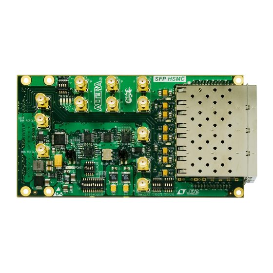
Furthermore, the SFP HSMC board is intended for customers to implement both telecommunication and data communications applications. 1.1 Features Figure 1.1 shows the photo of the SFP HSMC board. The important features are listed below: 8 SFP Connectors ... -
Page 4: About The Kit
1.2 About the KIT This section describes the package content SFP HSMC Board x 1 System CD-ROM x 1 The CD contains technical documents of the SFP HSMC, and reference designs along with the source code. Figure 1.2 SFP HSMC Package... -
Page 5: Assemble The Sfp Hsmc Board
Introduction 1.3 Assemble the SFP HSMC Board This section describes how to connect the SFP HSMC board to a main board. The SFP HSMC board connects with Altera DE3 Board... - Page 6 The SFP HSMC connects to the Stratix IV GX FPGA Development Board The SFP HSMC board connects with Altera Stratix III FPGA Deveopment Kit Note. Do not attempt to connect/remove the SFP HSMC daughter board to/from the main board when the power is on, or else the hardware could be damaged.
-
Page 7: Getting Help
Introduction 1.4 Getting Help Here are some places to get help if you encounter any problem: Email to support@terasic.com Taiwan & China: +886-3-550-8800 Korea : +82-2-512-7661 Japan: +81-428-77-7000... -
Page 8: Architecture
This Chapter covers the architecture of the SFP HSMC board including its PCB and block diagram. 2.1 Layout and Componets The picture of the SFP HSMC board is shown in Figure 2.1 and Figure 2.2. It depicts the layout of the board and indicates the location of the connectors and key components. - Page 9 Architecture Figure 2.2. The SFP HSMC Back side – HSMC connector view The following components are provided on the SFP HSMC board : LVDS SFP[4-7] (J10), XCVR SFP Dip Switch (S5), XCVR LVDS Dip Switch (S4), CLK2_SMA_p (J14), CLK2_SMA_n (J15), SMA_CLK1 (J9), PLL 4:1 Input Multiplexer Dip Switch (S3), PLL 4:1 Input...
-
Page 10: Block Diagram
Architecture 2.2 Block Diagram Figure 2.3 shows the block diagram of the SFP HSMC board Figure 2.3. The block diagram of the SFP HSMC board... -
Page 11: Board Components
All the control and data signals of the SFPs are connected to the HSMC connector, so users can fully control the SFP HSMC daughter board through the HSMC interface. Power is derived from 3.3V and 12V of the HSMC connector. - Page 12 Board Components Figure 3.1. The pin-outs on the HSMC connector...
- Page 13 Board Components The table 3.1 below lists the HSMC signal direction and description. Name Direction Description Numbers N.C. Not Connect N.C. Not Connect N.C. Not Connect N.C. Not Connect N.C. Not Connect N.C. Not Connect N.C. Not Connect N.C. Not Connect N.C.
- Page 14 Board Components N.C. Not Connect JTAG_TDO_TDI Inout JTAG data loop through JTAG_TDO_TDI Inout JTAG data loop through N.C. Not Connect N.C. Not Connect SEL[0] Inout CLK 1 Select bit 0 SEL[1] Inout CLK 1 Select bit 1 SEL[2] Inout CLK 2 Select bit 2 SEL[3] Inout CLK 2 Select bit 3...
- Page 15 Board Components SFP1_RATESEL Output Rate Select Power Power 3.3V Power Power 12V SFP1_LOS Input Receiver Loss of Signal Indication SFP0_TXFAULT Input Module Transmitter Fault SFP0_TXDISABLE Output Transmitter Disable, Turns off transmitter laser output SFP0_MOD2_SDA Inout SDA Serial Data Signal Power Power 3.3V Power Power 12V...
- Page 16 Board Components Power Power 12V SFP5_TDp Output Transmitter Non-Inverted Data Input SFP5_RDp Input Receiver Non-Inverted Data Output SFP5_TDn Output Transmitter Inverted Data Input SFP5_RDn Input Receiver Inverted Data Output Power Power 3.3V Power Power 12V SFP5_MOD1_SCL Output SCL Serial Clock Signal SFP5_MOD0_PRSNTn Input Not Connect...
-
Page 17: Clock Circuitry
Board Components SFP7_MOD2_SDA Inout SDA Serial Data Signal SFP7_MOD1_SCL Output SCL Serial Clock Signal SFP7_MOD0_PRSNTn Input LED indicator that the module is present Power Power 3.3V Power Power 12V SFP7_RATESEL Output Rate Select CLK2_p Input Differential Clock Input SFP7_LOS Input Receiver Loss of Signal Indication CLK2_n Input... - Page 18 Board Components Figure 3.2 Clock Diagram Table 3.2 CLK1 Settings SEL [1:0] CLK1p/CLK1n Frequency 125.00 MHz (Default) 155.52 MHz 156.25 MHz 61.44 MHz Table 3.3 CLK2 Settings SEL [3:2] CLK2p/CLK2n Frequency 125.00 MHz (Default) 155.52 MHz 156.25 MHz SMA_CLK_p/n...
-
Page 19: Power Supply
This section describes the power supply on the SFI HSMC board The SFP HSMC is powered through the HSMC connector’s 3.3V and 12V pins. The SFP and clocking circuitry requires 3.3V. A switching regulator powered from the 12 HSMC input produces 4V. Three linear regulators powered from 4V will produce the 3.3V. -
Page 20: Demonstration
SFP HSMC daughter board and the Stratix IV GX FPGA Development board. The demonstration is intended for users to provide a basic introduction to the SFP HSMC daughter board with the procedure to control different hardware and software settings. - Page 21 Demonstration Figure 4.3 Transceiver Loopback Test Setup Figure 4.4 LVDS Loopback Test Setup Note: The SFP HSMC board must be connected to HSMC Slot “B” of the Stratix IV GX FPGA Development Board for this demonstration...
-
Page 22: Demo Operation
Bit Stream used: hsmc_loopback.sof SFP HSMC Setup Insert SFP modules with loopback connectors into SFP ports 0-3 on the SFP HSMC board Set SW5 switches on the SFP HSMC all to the “0” position Stratix IV GX FPGA Development Kit Setup ... -
Page 23: Overview
HSMB_TX_P/N[3:0] of the Stratix IV GX device at 6.25Gbps. These high-speed serial data are then looped back through an external SFP HSMC back to the Stratix IV GX device. Through the SFP HSMC board the data is then equalized, retimed, deserialized, word aligned, 8B/10B decoded, channel bonded, and then the four bonded channels are compared against a receive side PRBS generator inside the Stratix IV GX FPGA fabric. - Page 24 Demonstration Figure 4.5 SFP Transceiver Test Block Diagram Transceiver/LVDS Loopback Definitions RESET – Resets the Board Test System PB0 – Enable Comma Detect PB1 – Enable Channel Bond PB2 – Start Transmitting PRBS data PB1 & PB2 – Pressing PB1 and PB2 at the same time creates and error in the transmitter data stream USER_LED[0] –...
-
Page 25: Appendix
April 20 , 2013 Modify some board name 5.2 Always Visit SFP HSMC Webpage for New Main board We will be continuing providing interesting examples and labs on our SFP HSMC webpage. Please visit www.altera.com or hsmcsfp.terasic.com for more information. - Page 26 Mouser Electronics Authorized Distributor Click to View Pricing, Inventory, Delivery & Lifecycle Information: Terasic P0040...
Need help?
Do you have a question about the SFP HSMC and is the answer not in the manual?
Questions and answers