Table of Contents
Advertisement
Quick Links
Advertisement
Table of Contents

Related Manuals for Terasic XTS-FMC


Summary of Contents for Terasic XTS-FMC
-
Page 2: Table Of Contents
3.2 Programmable Clock Generator......................14 Chapter 4 Demonstrations ......................15 4.1 XTS-FMC Loopback on the TR5 ..................... 15 4.2 XTS-FMC Loopback on the Han Pilot Platform ................19 4.3 XTS-FMC SuperLite Loopback on the Han Pilot Platform.............. 21 Appendix Revision History ............................. 24 XTS-FMC User www.terasic.com... -
Page 3: Chapter 1 Introduction
FPGA through the FMC connector. The XTS-FMC daughter card is the ideal platform to allow users to prototype and test their high-speed interfaces quickly and easily in support of transceiver performance for jitter, protocol compliance, and equalization. -
Page 4: The Package Contents
XTS-FMC Daughter Card Screw & Copper Pillar Package CD Download Guide The system CD contains technical documents of the XTS-FMC card, which include component datasheets, demonstrations, schematic and user manual. Users can download the CD from the link below: http://xts-fmc.terasic.com/cd www.terasic.com... -
Page 5: Assemble Xts-Fmc With Fpga Main Board
Figure 1-2 The contents of the XTS-FMC card. In order to make the XTS-FMC daughter card and the FMC connector on the FMC card with more secure hookup, the FMC side of the XTS-FMC daughter card has reserved two screw holes, as... -
Page 6: Getting Help
Secure the XTS-FMC on the FPGA main board Figure 1-4 Here are the addresses where you can get help if you encounter any problems: Terasic Technologies 9F., No.176, Sec.2, Gongdao 5th Rd, East Dist, Hsinchu City, 30070. Taiwan Email: support@terasic.com Tel.: +886-3-575-0880... -
Page 7: Chapter 2 Board Specification
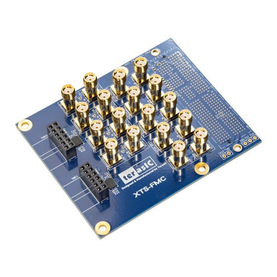
Chapter 2 Board Specification This chapter describes the architecture of the XTS card including block diagram and components. The picture of the XTS-FMC card is shown in Figure 2-1 Figure 2-2. It depicts the layout of the board and indicates the locations of the connectors and key components. -
Page 8: Block Diagram
Figure 2-2 Mechanical Layout of the XTS-FMC card The following components are provided on the XTS-FMC card: • FMC expansion connector (J11) • TX SMAs (J17/J19,J21/J23,J25/J26,J29/J31) • RX SMAs (J16/J18,J20/J22,J24/J27,J28/J30) • XCVR reference input SMAs (J12/J13) Figure 2-3 is the block diagram of the XTS-FMC card. - Page 9 Figure 2-3 Block diagram of the XTS-FMC card www.terasic.com XTS-FMC User Manual June 26, 2019...
-
Page 10: Mechanical Specifications
Figure 2-3 is the mechanical layout of the XTS-FMC board. Figure 2-4 The mechanical layout of the XTS-FMC card www.terasic.com XTS-FMC User Manual June 26, 2019... -
Page 11: Board Components
This chapter will describe the detailed information of the components, connector interface, and the pin mappings on the XTS-FMC card. The XTS-FMC card contains an FPGA Mezzanine Card (FMC) connector. All the other interfaces on the XTS-FMC card are connected to the FMC connector. - Page 12 Figure 3-2 Signal names of XTS-FMC connector part 2 Figure 3-3 Signal names of XTS-FMC connector part 3 www.terasic.com XTS-FMC User Manual June 26, 2019...
- Page 13 Figure 3-4 Signal names of XTS-FMC connector part 4 Table 3-1 FMC Pin Assignments Signal Name FMC Pin Direction I/O Standard Description XCVR_TX0_p PIN_C2 Output 1.4-V PCML Transceiver Output Port0, connected to J17(SMA) XCVR_TX0_n Transceiver Output Port0, PIN_C3 Output 1.4-V PCML...
- Page 14 CDCM6208. FMC_I2C_SDA PIN_C31 Inout VCCADJ I2C data bus for the clock generator CDCM6208 FMC_I2C_SCL I2C clock bus for the clock generator PIN_C30 Ouput VCCADJ CDCM6208 www.terasic.com XTS-FMC User Manual June 26, 2019...
-
Page 15: Programmable Clock Generator
The XTS-FMC card provides a programmable clock generator: CDMC6208. This clock generator provides a variety of frequencies which can have different formats to the FPGA's transceiver bank for different applications as reference clock. The user can modify the output frequency of DMC6208 from the FPGA through the I2C interface. -
Page 16: Chapter 4 Demonstrations
The transceiver test code is available in the folder System CD\Demonstrations\TR5\demo_batch. Here are the procedures to perform transceiver channel test: Use the SMA cables to connect the TX ports and the RX ports on the XTS-FMC card to implement the loopback function (See Figure 4-1, Figure 4-2). - Page 17 Connect the XTS-FMC card to the FMC D or FMC A connector of the TR5 board. Make sure the FMC connector between the two boards is locked with copper posts and screws (See section 1.3). Figure 4-2 The Connections between the XTS-FMC card and TR5 board Connect your TR5 board to your PC with a mini USB cable.
- Page 18 Figure 4-3 Choose the Test function Then enter how many seconds you want to test the transmission (See Figure 4-4). For example, enter “60” for test 60 second. www.terasic.com XTS-FMC User Manual June 26, 2019...
- Page 19 FMC A and FMC D connectors on the TR5 board (8 pairs of transceivers for each connector). Since XTS-FMC card can only test 4 pairs of transceivers. So the test result will only show the first four transceivers (0~3) of FMC A or FMC D are PASS or NG.
-
Page 20: Xts-Fmc Loopback On The Han Pilot Platform
The transceiver test code is available in the folder System CD\Demonstrations\HAN\XCVT loopback. Here are the procedures to perform transceiver channel test: Use the SMA cables to connect the TX ports and the RX ports on the XTS-FMC card to implement the loopback function (See Figure 4-6). - Page 21 When the menu option appears, you can choose 0 for starting test. The program will automatically start the test and report the test results every five seconds until the user closes the window (see Figure 4-8). Figure 4-7 The test program www.terasic.com XTS-FMC User Manual June 26, 2019...
-
Page 22: Xts-Fmc Superlite Loopback On The Han Pilot Platform
The transceiver test code is available in the folder System CD\Demonstrations\HAN\ SuperLite Loopback\demo_batch. Here are the procedures to perform transceiver channel test: 1. Use the SMA cables to connect the TX ports and the RX ports on the XTS-FMC card to implement the loopback function (See Figure 4-9). - Page 23 Figure 4-9 The Connections between the XTS-FMC and HAN Pilot Platform board 3. Connect your HAN board to your PC with a mini USB cable. 4. Connect Power to the HAN Pilot Platform board. 5. Copy the demo_batch folder (from System CD) to your local disk.
- Page 24 PMA parameters. Based on our actual experiment, we provided a group of PMA parameters as shown in Table 4-1, user can modify the PMA parameters by referring the values in . Table 4-1 PMA parameters based on our actual experiment PostTap PreTap other Default www.terasic.com XTS-FMC User Manual June 26, 2019...
-
Page 25: Appendix
Appendix Version Change Log V1.0 Initial Version (Preliminary) V1.1 Add section 2.3 V1.2 Add section 4.3 Copyright © Terasic Inc. All rights reserved. XTS-FMC User www.terasic.com Manual June 26, 2019...
Need help?
Do you have a question about the XTS-FMC and is the answer not in the manual?
Questions and answers