Table of Contents
Advertisement
Quick Links
Advertisement
Table of Contents

Related Manuals for Terasic XTS-FMC


Summary of Contents for Terasic XTS-FMC
-
Page 2: Table Of Contents
3.1 FMC Expansion Connector ....................... 10 Chapter 4 Demonstrations ......................14 4.1 XTS-FMC Loopback on the TR5 ..................... 14 4.2 XTS-FMC Loopback on the Han Pilot Platform ................18 4.3 XTS-FMC SuperLite Loopback on the Han Pilot Platform.............. 20 Appendix Revision History ............................. 23 www.terasic.com... -
Page 3: Chapter 1 Introduction
FPGA transceiver signals can be easily connected to measurement instruments as well as allowing gigabit data rate communication between multiple FPGA boards. The XTS-FMC daughter card is the ideal platform to allow users to prototype and test their high-speed interfaces quickly and easily in support of transceiver performance for jitter, protocol compliance, and equalization. -
Page 4: The Package Contents
Figure 1-2 The contents of the XTS-FMC card. In order to make the XTS-FMC daughter card and the FMC connector on the FMC card with more secure hookup, the FMC side of the XTS-FMC daughter card has reserved two screw holes, as... - Page 5 Figure 1-3 The two screw holes on XTS-FMC card. Secure the XTS-FMC on the FPGA main board Figure 1-4 www.terasic.com XTS-FMC User Manual January 2, 2020...
-
Page 6: Getting Help
Here are the addresses where you can get help if you encounter any problems: Terasic Technologies 9F., No.176, Sec.2, Gongdao 5th Rd, East Dist, Hsinchu City, 30070. Taiwan Email: support@terasic.com Tel.: +886-3-575-0880 Website: xts-fmc.terasic.com www.terasic.com XTS-FMC User Manual January 2, 2020... -
Page 7: Chapter 2 Board Specification
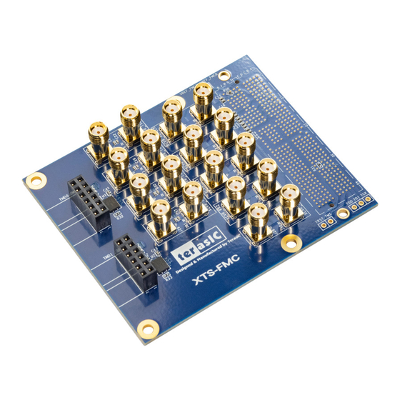
Chapter 2 Board Specification This chapter describes the architecture of the XTS card including block diagram and components. The picture of the XTS-FMC card is shown in Figure 2-1 Figure 2-2. It depicts the layout of the board and indicates the locations of the connectors and key components. -
Page 8: Block Diagram
Figure 2-2 Mechanical Layout of the XTS-FMC card The following components are provided on the XTS-FMC card: FMC expansion connector (J11) TX SMAs (J17/J19,J21/J23,J25/J26,J29/J31) RX SMAs (J16/J18,J20/J22,J24/J27,J28/J30) XCVR reference input SMAs (J12/J13) Figure 2-3 is the block diagram of the XTS-FMC card. -
Page 9: Mechanical Specifications
Figure 2-3 Block diagram of the XTS-FMC card Figure 2-3 is the mechanical layout of the XTS-FMC board. www.terasic.com XTS-FMC User Manual January 2, 2020... - Page 10 Figure 2-4 The mechanical layout of the XTS-FMC card www.terasic.com XTS-FMC User Manual January 2, 2020...
-
Page 11: Chapter 3 Board Components
This chapter will describe the detailed information of the components, connector interface, and the pin mappings on the XTS-FMC card. The XTS-FMC card contains an FPGA Mezzanine Card (FMC) connector. All the other interfaces on the XTS-FMC card are connected to the FMC connector. - Page 12 Figure 3-2 Signal names of XTS-FMC connector part 2 Figure 3-3 Signal names of XTS-FMC connector part 3 www.terasic.com XTS-FMC User Manual January 2, 2020...
- Page 13 Figure 3-4 Signal names of XTS-FMC connector part 4 Table 3-1 FMC Pin Assignments Signal Name FMC Pin Direction FMC Pin I/O Standard Description XCVR_TX0_p SMA Transceiver PIN_C2 Output DP_C2M_P0 1.4-V PCML Output Port0, connected to J17(SMA) XCVR_TX0_n PIN_C3 Output DP_C2M_N0 1.4-V PCML...
- Page 14 1.4-V PCML Input Port3, connected to J30(SMA) XCVR_REFCL PIN_D4 Input GBTCLK_M2C LVDS External reference K0_p clock input, connected to J12(SMA) XCVR_REFCL PIN_D5 Input GBTCLK_M2C LVDS External reference K0_n clock input, connected to J13(SMA) www.terasic.com XTS-FMC User Manual January 2, 2020...
-
Page 15: Chapter 4 Demonstrations
The transceiver test code is available in the folder System CD\Demonstrations\TR5\demo_batch. Here are the procedures to perform transceiver channel test: Use the SMA cables to connect the TX ports and the RX ports on the XTS-FMC card to implement the loopback function (See Figure 4-1, Figure 4-2). - Page 16 Connect the XTS-FMC card to the FMC D or FMC A connector of the TR5 board. Make sure the FMC connector between the two boards is locked with copper posts and screws (See section 1.3). Figure 4-2 The Connections between the XTS-FMC card and TR5 board Connect your TR5 board to your PC with a mini USB cable.
- Page 17 Figure 4-3 Choose the Test function Then enter how many seconds you want to test the transmission (See Figure 4-4). For example, enter “60” for test 60 second. www.terasic.com XTS-FMC User Manual January 2, 2020...
- Page 18 FMC A and FMC D connectors on the TR5 board (8 pairs of transceivers for each connector). Since XTS-FMC card can only test 4 pairs of transceivers. So the test result will only show the first four transceivers (0~3) of FMC A or FMC D are PASS or NG.
-
Page 19: Xts-Fmc Loopback On The Han Pilot Platform
The transceiver test code is available in the folder System CD\Demonstrations\HAN\XCVT loopback. Here are the procedures to perform transceiver channel test: Use the SMA cables to connect the TX ports and the RX ports on the XTS-FMC card to implement the loopback function (See Figure 4-6). - Page 20 When the menu option appears, you can choose 0 for starting test. The program will automatically start the test and report the test results every five seconds until the user closes the window (see Figure 4-8). Figure 4-7 The test program www.terasic.com XTS-FMC User Manual January 2, 2020...
-
Page 21: Xts-Fmc Superlite Loopback On The Han Pilot Platform
The transceiver test code is available in the folder System CD\Demonstrations\HAN\ SuperLite Loopback\demo_batch. Here are the procedures to perform transceiver channel test: 1. Use the SMA cables to connect the TX ports and the RX ports on the XTS-FMC card to implement the loopback function (See Figure 4-9). - Page 22 Figure 4-9 The Connections between the XTS-FMC and HAN Pilot Platform board 3. Connect your HAN board to your PC with a mini USB cable. 4. Connect Power to the HAN Pilot Platform board. 5. Copy the demo_batch folder (from System CD) to your local disk.
- Page 23 PMA parameters. Based on our actual experiment, we provided a group of PMA parameters as shown in Table 4-1, user can modify the PMA parameters by referring the values in . Table 4-1 PMA parameters based on our actual experiment PostTap PreTap other Default www.terasic.com XTS-FMC User Manual January 2, 2020...
-
Page 24: Appendix
Appendix Version Change Log V1.0 Initial Version (Preliminary) V1.1 Add section 2.3 V1.2 Add section 4.3 V2.0 Modify by XTS-FMC Rev B board Copyright © Terasic Inc. All rights reserved. www.terasic.com XTS-FMC User Manual January 2, 2020...
Need help?
Do you have a question about the XTS-FMC and is the answer not in the manual?
Questions and answers