Table of Contents
Advertisement
Quick Links
Advertisement
Table of Contents

Related Manuals for Motorola PPC/PMC-8260/DS1


Summary of Contents for Motorola PPC/PMC-8260/DS1
- Page 1 PPC/PMC-8260/DS1 Reference Guide P/N 6806800B10A July 2006...
- Page 2 Motorola reserves the right to revise this document and to make changes from time to time in the content hereof without obligation of Motorola to notify any person of such revision or changes.
-
Page 3: Table Of Contents
Ordering Information ..........8 PPC/PMC-8260/DS1... - Page 4 FCC Requirements for PPC/PMC-8260/DS1 ........
- Page 5 Resetting the PPC/PMC-8260/DS1 ........
- Page 6 Motorola PowerQUICC II ........
- Page 7 Configuring the PPC/PMC-8260/DS1 as Clock Master ........
- Page 8 PPC/PMC-8260/DS1...
- Page 9 PPC/PMC-8260/DS1 on Reference Platforms ........
- Page 10 Used Port Pins of SI2 ............12 PPC/PMC-8260/DS1...
- Page 11 Firmware Figure 12 Flowchart of the PPC/PMC-8260/DS1 Firmware Power-Up Sequence ....5 Figure 13 Memory Layout of the Primary Booter ........16...
- Page 12 Connection of Data Lines in Inter-TDM Link ....... . . 10 PPC/PMC-8260/DS1...
-
Page 13: Using This Guide
Typical notation used for variables and keys [text] Typical notation for buttons Repeated item Ranges Extents No danger encountered. Pay attention to important information marked using this layout Note: Caution Possibly dangerous situation: slight injuries to people or damage to objects possible PPC/PMC-8260/DS1 xiii... - Page 14 Control/Status Register Channel Service Unit Direct Memory Access DRAM Dynamic Random Access Memory Electromagnetic Compatibility Electrostatic Discharge Field Applications Engineer Federal Communications Commission Ground GPCM General-Purpose Chip-Select Module GPIO General Purpose Input/Output Integrated Circuit In-Circuit Tester IDMA Independent DMA PPC/PMC-8260/DS1...
- Page 15 Message Transfer Protocol Processor Bus Printed Circuit Assembly Peripheral Component Interconnect Pulse Code Modulation Power-Up Control Register PCI Mezzanine Card POST Power-On Self Test POST Result Code PROM Programmable Read-Only Memory PSDVAL Partial Data Valid Power-up Status Register Random Access Memory PPC/PMC-8260/DS1...
- Page 16 Synchronous Static Random Access Memory SYPCR System Protection Control register Transfer Acknowledge Test Data In Time Division Multiplex Test Data Out Telecommunication Network Voltage Time Slot Assigner Test Status Register User-programmable Machine Versa Module Eurocard PCI Vital Product Data PPC/PMC-8260/DS1...
- Page 17 Feedback Motorola welcomes and appreciates your comments on its documentation. We want to know what you think about our manuals and how we can make them better. Mail comments to: • Motorola GmbH ECC Embedded Communication Computing Lilienthalstr. 15 85579 Neubiberg-Munich/Germany •...
-
Page 18: Revision History
PMC-8260/DS1-H.110-RLH”; Added note to the "JTAG/Debug” section; Removed Troubleshooting chapter; Added the "Appendix” chapter; 215165 August 2001 Added the the "Index” section Editorial changes; 215165 November 2001 Editorial changes: removed picture from title page, corrected document number xviii PPC/PMC-8260/DS1... -
Page 19: Features
12 "JTAG/Debug Connector Pinout” ; deleted figure "Local TDM Streams Structure on PMC- 8260/DS1-N-(R/F) Variant”; completely revised the "Firmware” chapter; completely revised the "Memory Map and Devices” chapter; completely revised the former "Structuresî chapter and renamed to "TDM Channel Configuration PPC/PMC-8260/DS1... -
Page 20: Variants
PCI bus and signaling level information to the "Installing a PMC Module” section; modified Figure 15 "Block Diagram” 222192 May 2006 Brought manual to Motorola-style (copyright, logo, etc.) 6806800B10 July 2006 Changed email address for reader comments in section “Feedback”... -
Page 21: Other Sources Of Information
IEEE Standard Physical and Environmental Layers for PCI Mezzanine Cards (PMC) - IEEE1386.1- 2001 Micron micron.com MT48LC4M16A2 and MT48LC8M16A2 (SDRAM) MT58L256L36F-S-10 (SSRAM) PMC-Sierra pmc-sierra.com PMC-Sierra PM4351 (COMET) Tundra tundra.com PowerSpan II ™ PowerPC-to-PCI Bus Switch User Manual PowerSpan II and PowerSpan Differences Summary PPC/PMC-8260/DS1... - Page 22 PPC/PMC-8260/DS1...
-
Page 23: Safety Notes
The module has been tested in a standard Motorola system and found to com- ply with the limits for a Class A digital device in this system, pursuant to part 15 of the FCC Rules respectively EN 55022 Class A. - Page 24 (the “Allowed Product Combinations” section page 2-8). Otherwise damage to PMC module or the carrier board may occur. The PPC/PMC-8260/DS1 is not certified for the use with TNV-1 circuits (Telecommunication Network Voltage-1 circuits). Do not connect E1/T1/J1 lines directly to the PPC/PMC-8260/DS1. Use a Digital Service Unit/Control Service Unit (DSU/CSU) to eliminate overvoltages.
- Page 25 PMC module and to attached devices. Therefore, only connect E1/T1/J1 lines to the RJ-45 connector using a Digital Service Unit / Control Service Unit (DSU/CSU). Environment Always dispose of old modules according to your country’s legislation, if possi- ble in an environmentally acceptable way. PPC/PMC-8260/DS1...
- Page 26 PPC/PMC-8260/DS1...
- Page 27 Wartung des PPC/PMC-8260/DS1 zu beachten sind. Wir sind darauf bedacht, alle notwendigen Informationen zur Installation und zum Betrieb mit dem PPC/PMC-8260/DS1 in diesem Handbuch bereit zu stellen. Da es sich jedoch bei dem PPC/PMC-8260/DS1 um ein komplexes Produkt mit vielfältigen Einsatzmöglichkeiten handelt, können wir die Vollständigkeit der im...
- Page 28 (siehe Abschnitt “Allowed Product Combinations” auf Seite 2-8). Sonst können das PMC Modul oder die Trägerkarte beschädigt werden. Das PPC/PMC-8260/DS1 ist nicht für den Betrieb mit einer TNV-1 Spannung (Telecommunication Network Voltage-1 Spannung) zertifiziert. Verbinden Sie E1/T1/J1 nicht direkt mit der TNV-1 Spannung. Verwenden Sie eine Digital Service Unit/Control Service Unit (DSU/CSU), um Überspannungen zu ver-...
- Page 29 Luftfeuchtigkeit und Temperatur, da durch hohe Luft- feuchtigkeit und Kondensation Kurzschlüsse entstehen können. Stellen Sie vor dem Einschalten des Stroms sicher, dass sich auf dem PPC/PMC-8260/DS1 kein Kondensat befindet, und betreiben Sie das PPC/PMC-8260/DS1 nicht unter 0°C.
- Page 30 PPC/PMC-8260/DS1...
- Page 31 Introduction...
- Page 33 Combined with a CompactPCI or VME CPU carrier board, the PPC/PMC-8260/DS1 is an ideal platform for applications in areas such as Wireless Infrastructure, Unified Messaging Servers, Enterprise Computer Telephony, Intel- ligent Peripherals, and Advanced Intelligent Network.
-
Page 34: Function Blocks
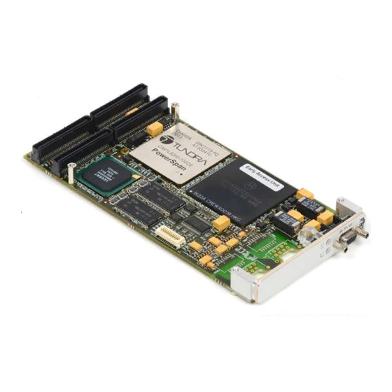
Features Introduction The PPC/PMC-8260/DS1 function blocks are shown in the figure below. Local Tundra SSRAM 32 Bit Motorola PCI Bus PowerSPAN II 1 MByte MPC8260 32-/64 bit, PCI Bridge 66 MHz 300 MHz 33/66MHz 33/66 MHz Framer Boot Flash SDRAM 64 Bit... -
Page 35: Restrictions
There are three different variants of the PPC/PMC-8260/DS1: • PMC-8260/DS1-SC-F • PMC-8260/DS1-H110-F The letter “F” stands for two line interfaces on the front panel. PMC-8260/DS1-SC-F The PMC-8260/DS1-SC-F is tailored to be mounted on the following Motorola carrier boards: • PowerCore-660x (VMEbus) • PowerCore-6750 (VMEbus) •... -
Page 36: Variant Features
The PMC-8260/DS1-H110-F variants have the following restrictions: • Front panel line interfaces of PMC-8260/DS1-H110-F variant only support short haul. • On the carrier boards, only PMC slot 2 is connected to the H.110 bus (Com- pactPCI P4 connector). 1 - 6 PPC/PMC-8260/DS1... -
Page 37: Standard Compliances
Introduction Standard Compliances Standard Compliances The PPC/PMC-8260/DS1 meets the following standard requirements: Table 1: Standard Compliances Standard Description EN 55024 EMC requirements on system level EN 55022 FCC Part 15 EN 60950-1 Legal safety requirements UL 60950-1 CAN/CSA C222 No 60950-1... -
Page 38: Ordering Information
• SC bus or H.110 bus support The variant of the PPC/PMC-8260/DS1 to be used depends on the carrier board (see the “Allowed Product Combinations” section on page 2-8). Consult your local sales representative to confirm availability of specific combinations. - Page 39 Installation...
-
Page 41: Action Plan
In order to install the PMC module, the following steps are necessary and are described in detail in the sections of this chapter. Start installation Make sure requirements are met Check if switch settings are correct Install PMC module Installation finished PPC/PMC-8260/DS1 2 - 3... -
Page 42: Environmental Requirements
8260/DS1 in a public network you need a CSU (channel service unit). Carrier Board Signaling Level Requirements The PPC/PMC-8260/DS1 supports signaling levels 3.3V and 5V and therefore is a universal PMC module. Make sure that your carrier board has a signaling level of 3.3V or 5V at the PMC interface. -
Page 43: Power Requirements
1200 mm/all edges and corners (packed state) Power Requirements The power supply must meet the power requirements of the carrier board and the PPC/PMC-8260/DS1 module. For the power requirements of the carrier board refer to the respective Installation Guide. Caution •... -
Page 44: Environmental Requirements Of The Ppc/Pmc-8260/Ds1
• The PMC specification (P1386.1) specifies a maximum total power con- sumption of 7.5W per PMC module. The PPC/PMC-8260/DS1 in its stan- dard configuration may exceed this value. Therefore, it is neccessary to synchronize the carrier board’s power supply with the PPC/PMC- 8260/DS1 power requirements. -
Page 45: Location Of Switch
Installation Switch Settings Switch Settings The PPC/PMC-8260/DS1 is configurable via switch SW1. 1 2 3 4 Figure 2: Location of Switch Note: • In normal operation mode SW1-1 must be in OFF position. If switch 1-1 is ON, the PMC module does not boot. -
Page 46: Allowed Product Combinations
Table 7 “Revisions Supported by Reference Platform” on page 2-9 Note: As described in the table above, the reference platform PowerCoreCP- CI-6750 Rev.2.x supports two PPC/PMC-8260/DS1 modules, depending on the hardware revision. The supported hardware revisions are listed in the fol- lowing table. - Page 47 Official Order Number vision Rev. L 106347 PCA PowercoreCPCI- 106476 PPC/PowerCoreCPCI-6750/ 6750/0-233-L512-4/R.2 64-233-L512-4 R2 Rev. M 106349 PCA PowercoreCPCI- 106477 PPC/PowerCoreCPCI-6750/ 6750/0-400-L1024-8R.2 128S-400-L1M-8 R2 106478 PPC/PowerCoreCPCI-6750/ 64S-400-L1M-8 R2 Rev. H 107398 PCA PowercoreCPCI- 107344 PPC/PowerCoreCPCI-6750/ 6750/0-500-L1M-8/2.0 128S-500-L1M-8R2 PPC/PMC-8260/DS1 2 - 9...
-
Page 48: Installing A Pmc Module
Installation Installing a PMC Module The PPC/PMC-8260/DS1 supports a data bus width of 32/64 bit with a frequency of 33 or 66 MHz. The supported signaling levels are 3.3V and 5V, therefore, the PPC/PMC-8260/DS1 can be installed on carrier boards with a signaling level of 3.3V or 5V at their PMC interface. -
Page 49: Installation Procedure
Installation Installation Procedure You can install the PPC/PMC-8260/DS1 on carrier boards with or without hot- swap support. If you install it on a hot-swappable carrier board, start installation procedure with step 4. If you install it on a non-hot-swap carrier board, start with step 1. -
Page 50: Figure 3 Installation (Example With Powercorecpci-6750 Rev. 2.X)
Figure 3: Installation (Example with PowerCoreCPCI-6750 Rev. 2.x) 9. Fasten four screws delivered with PMC module 10. Install carrier board according to carrier board’s Installation Guide 11. Attach interface cables 12. If not installing a hot-swappable carrier board, switch power on 2 - 12 PPC/PMC-8260/DS1... -
Page 51: Removal Procedure
4. Remove carier board from system according to carrier board’s Installa- tion Guide 5. Remove screws holding respective PMC module 6. Disconnect PMC module carefully from slot 7. Close front panel gap at free slot with blind panel PPC/PMC-8260/DS1 2 - 13... -
Page 52: Software Upgrades And Accessories
Installation Software Upgrades and Accessories Motorola provides software packages with control, configuration and test functions for the layer-2 protocols MTP-2, LAPD, and Frame Relay. Support is available for the operating systems Solaris 2.6, 2.7 and 8, VxWorks 5.4/Tornado 2.0 and Linux Kernel 2.4.x. - Page 53 Indicators and Connectors...
-
Page 55: Front Panels
Front Panel The interface connectors and LEDs available on the different variants can be seen in the following figure. Motorola Serial Interface User-Programmable LEDs Line Interfaces L1 L2 LINE 1 LINE 2 Figure 4: Front Panels PPC/PMC-8260/DS1 3 - 3... -
Page 56: Indicators And Connectors
Only available on board and used for CT-Bus Management Bus (CT_MC) SCC_3 (HDLC) SCC3 is clocked by T8105 clock output L_SC<0>=T8105_MC_CLK signal=2.048 MHz PowerQUICC II SCC_4 and SMC_2 are not connected to any external devices. SCC_4 and SMC_2 3 - 4 PPC/PMC-8260/DS1... -
Page 57: Front Panel Rj-45 Interface Connector Pinout
Front Panel RJ-45 Interface Connector Pinout LEDs The PPC/PMC-8260/DS1 offers two user-programmable LEDs L1 and L2 (for lo- cation see Figure 4 “Front Panels” on page 3-3) which can take the states “off”, “red”, “green” and “yellow”. At power up, they show the state of the power-up se- quence. - Page 58 Yellow T8105 test running Yellow POST complete Yellow Green Executing ROM image (end of boot sequence) Green Primary booter Idle loop Green (dimmed flashing) Flash erase/write operation Yellow (flashing) ongoing Before execution of uploaded Green image 3 - 6 PPC/PMC-8260/DS1...
-
Page 59: Pmc I/O And Jtag/Debug Connector
Indicators and Connectors On-Board Connectors On-Board Connectors Apart from the three standard PMC connectors, the PPC/PMC-8260/DS1 offers the PMC I/O and the JTAG/Debug connector. The figure below shows the location of these two connectors. JTAG/Debug Connector (P4) PMC I/O Figure 7:... -
Page 60: Figure 8 Pmc I/O Connector Pinout For Pmc-8260/Ds1-Sc-F
PMC I/O Connector Pinout for PMC-8260/DS1-SC-F Note: Pins 27, 29, 30, 31, and 32 available on the PMC/860...E1/T1 (SCBus ID pins) are not available on the PPC/PMC-8260/DS1. Otherwise pin compatibil- ity is given between PMC/860...E1/T1 and PPC/PMC-8260/DS1. 3 - 8... -
Page 61: Figure 9
BTCLK_PMC_IN* BTCLK_PMC_OUT* BTFP_PMC_IN* BTFP_PMC_OUT* PQ2_C2_L1RXD_IN* T8105_LDO<10>* PQ2_D2_L1RXD_IN* T8105_LDO<11>* n.c. FET_CTRL_B n.c. EARLY_PMC PQ2_C2_L1TXD_OUT* T8105_LDI<10>* PQ2_D2_L1TXD_OUT* T8105_LDI<11>* Figure 9: PMC I/O Connector Pinout for PMC-8260/DS1-H110-F Note: The signals marked by an asterisk are inter-TDM link signals. PPC/PMC-8260/DS1 3 - 9... -
Page 62: Figure 10 Jtag/Debug Connector
Note: The COP interface is not available on revisions prior to Revision 1.2. The JTAG/Debug connector provides the signals of the PowerQUICC II COP in- terface port which allows easy connection of a Standard Motorola Third Party COP-Interface Emulator. Additionally, it provides a second RS-232 interface for debugging convenience (PowerQUICC II SMC1-interface) and the necessary sup- ply voltages. -
Page 63: Figure 11 Jtag/Debug Connector Pinout
The JTAG/Debug connector is a two-row 21-pin SMD connector (vertical recepti- ble of the type BERG CONAN 91931-WXY21) with 1 mm pin-pitch located on the bottom side of the PPC/PMC-8260/DS1 module (see Figure 10 “JTAG/Debug Connector” on page 3-10). The following figure shows the pinout of the JTAG/Debug mode connector. - Page 64 On-Board Connectors Indicators and Connectors 3 - 12 PPC/PMC-8260/DS1...
- Page 65 Firmware...
-
Page 67: Introduction
– Load application software via PCI bus – Program application software into the boot flash device – Read from and write to all devices on the PPC/PMC-8260/DS1 – Obtain detailed results from the power-on self-test to evaluate error condi- tions •... -
Page 68: Power-Up Sequence
Only the front panel LEDs show the current status of the boot process, the power-on self-test and the primary booter (see Table 9 “LED States During Power Up” page 3-5). 4 - 4 PPC/PMC-8260/DS1... -
Page 69: Figure 12 Flowchart Of The Ppc/Pmc-8260/Ds1 Firmware Power-Up Sequence
Firmware Power-Up Sequence Figure 12: Flowchart of the PPC/PMC-8260/DS1 Firmware Power-Up Sequence PPC/PMC-8260/DS1 4 - 5... -
Page 70: Table 10 Steps Performed During Power-Up
(see the “Obtaining Results from the Power-On Self-Test” section on page 4-24). Disable POST If the POST is completed, the firmware sets the PSKIP bit in the PCR register so that the POST is not executed again after a warm start. 4 - 6 PPC/PMC-8260/DS1... - Page 71 PSR. This information can be used to poll the power-up status. Set power-up status (PSR) to Before the primary booter is started, the value 2 is written into the PSR. This status bit can be used to poll the power-up status. PPC/PMC-8260/DS1 4 - 7...
-
Page 72: Loading Application Software
– Reading and writing to I/O devices – Optional: Reading POST results If you use the Tornado 2.0 BSP for the PPC/PMC-8260/DS1 such a driver is al- ready implemented. For more information on the BSP, refer to the BSP documenta- tion. -
Page 73: Preparing A Rom Image
You can, for example, define the SYPCR register value, POST execution speed and whether POST is executed or not. The following table shows the offsets and values to be programmed. PPC/PMC-8260/DS1 4 - 9... -
Page 74: Table 11 Rom Image Configuration Section
1: Fast POST SHADOW RAM shadow 0: No shadow to RAM is executed 1: Shadow to RAM is executed SMODE Shadow incl. configura- tion section 0: Shadow without con- figuration section 1: Shadow with configu- ration section 4 - 10 PPC/PMC-8260/DS1... -
Page 75: Argument Passed To Rom Image
[ to RAM_ADRS If SYPCR_WR is 0 Write SYPCR_VAL to SYPCR register Set LEDs to GREEN/OFF If RAM_EXEC is within the address range of the copied image Jump to RAM address RAM_EXEC else Jump to RAM_ADRS+108 PPC/PMC-8260/DS1 4 - 11... -
Page 76: System State At Rom Image Execution
Port Pin Configuration The firmware does not program the pin assignment registers for ports A-C. If you have purchased the Motorola Tornado 2.0 BSP for the PPC/PMC-8260/DS1 or one of the Motorola stackware packages, you do not need to program the PowerQUICC II port pins. -
Page 77: Table 12 Pcr Register Settings
1: Software watchdog timer will be disabled. It is not possible to enable the software watchdog timer once it has been disabled except by resetting PPC/PMC-8260/DS1. In any case, the firmware will periodically trigger the software watchdog to prevent it from expiring. -
Page 78: Monitoring Boot Process
• 3 (ROMEX) This value is set after all initialization steps and optionally the POST are com- pleted and a ROM image has been detected and is about to be executed. 4 - 14 PPC/PMC-8260/DS1... -
Page 79: Primary Booter
PCI bus (left). The SDRAM and SSRAM regions marked by the dashed lines are not directly accessible from PCI bus. In order to read from/write to these regions, the contents must first be copied into the I/O buffer area (see shaded area in the following figure). PPC/PMC-8260/DS1 4 - 15... -
Page 80: Table 13 Primary Booter Csr Section
For a list of available commands, see Table 14 “Pri- mary Booter Commands and Parameters” page 4-18. ADRS Argument for SYNC This parameter is used for the .go! command to indicate at which local memory address to start program execu- tion. 4 - 16 PPC/PMC-8260/DS1... - Page 81 Reserved CADR Source or destination address CSIZ Number of bytes to be transferred PSTAT POST Result: 0: POST passed 1: POST failed Reserved PINFO see Table 16 “POST Result and Status Bits” page 4-25 PPC/PMC-8260/DS1 4 - 17...
-
Page 82: Table 14 Primary Booter Commands And Parameters
Unless the primary booter is busy with the previous operation, it will set the .OK. status immediately as it sees PING. For a code example, see the “Checking Alive State of Target” sec- tion on page 4-37. 4 - 18 PPC/PMC-8260/DS1... - Page 83 0 can be interpreted as offset relative to the beginning of the CSR section where a zero-terminated error string is stored. • <Written SYNC word> Primary booter either does not support the command or some error prevents the PPC/PMC-8260/DS1 4 - 19...
-
Page 84: Starting The Primary Booter
8. Deassert reset from local CPU by clearing pending mailbox interrupt After resetting the PPC/PMC-8260/DS1 it should not take more than one sec- ond for the PSR to be set either to RDY or POST. When POST is set, it should... - Page 85 Firmware Loading Application Software PPC/PMC-8260/DS1). If it takes longer than 16 seconds for RDY to be set, a firmware or hardware error occured and the PMC module has to be sent back to Motorola. 9. Poll PSR register until RDY value appears After the RDY status is read, it should not take more than one second for the primary booter to assert either “.OK.”...
-
Page 86: Reading And Writing
Firmware Reading and Writing Only part of the address space of the PPC/PMC-8260/DS1 is directly accessible from the PCI bus (see the “Resources Used by the Primary Booter” section on page 4-15). The other parts of the address map (e.g. boot flash area) can be accessed by using the read and write command sequence. -
Page 87: Programming A Boot Image Into Boot Flash
7. Start operation by writing command “flsh” into SYNC field 8. Wait for completion (see the “Return Codes” section on page 4-19) 1) Using the primary booter for programming the boot flash requires also a programming routinge for start- ing the primary booter. PPC/PMC-8260/DS1 4 - 23... -
Page 88: Obtaining Results From The Power-On Self-Test
The POST stores information on its progress and the results in bank 12 of the inter- nal dual-ported RAM of the PowerQUICC II. The offset relative to the IMMR is B800 , resulting in the absolute address of F000B800 in the memory map of the PPC/PMC-8260/DS1. 4 - 24 PPC/PMC-8260/DS1... -
Page 89: Table 15 Post Result Storage Area
Set to 1 if framer #3 passed all tests Set to 1 if framer #4 passed all tests Set to 1 if the T8105 passed all tests Set to 1 if the PowerSpan II PCI bridge passed all tests PPC/PMC-8260/DS1 4 - 25... -
Page 90: Checksum
Each bit set in one of these words indicates a specific operation which failed. In general, a test result word of FFFFFFFF indicates a device that is either not as- sembled or could not be accessed. Only the latter case is indicated as error in the PRC. 4 - 26 PPC/PMC-8260/DS1... -
Page 91: Table 18 Synchronous Sram Test
The assembled SSRAM size as determined by probing is not supported. 4...30 Memory pattern test failed. The index of the long-WORD which failed the test is stored in bits 4...31 (i.e. shifted by four), beginning with 1 for the first address. Fatal error during test execution PPC/PMC-8260/DS1 4 - 27... - Page 92 Data mismatch when accessing register at offset 0 Data mismatch when accessing register at offset FF Data mismatch when writing 55 to register FE Data mismatch when writing AA to register FE Fatal error during test execution 4 - 28 PPC/PMC-8260/DS1...
- Page 93 Wrong device ID (CSR register at offset FE Data mismatch when writing 55 to the first byte of CAM Data Memory 1 Data mismatch when writing AA to the first byte of CAM Data Memory 1 Fatal error during test execution PPC/PMC-8260/DS1 4 - 29...
-
Page 94: Code Examples
Code Examples This section contains C code examples which can be implemented into your driver software to enable communication between the host and the PPC/PMC-8260/DS1 firmware via the PCI bus. It assumes that the PowerSpan II PCI bridge has been fully initialized by the host’s PCI enumerator and is accessible. - Page 95 /* -> high */ #define PB_HDR_CP_CADRL (0x000000ac) /* -> low*/ #define PB_HDR_CP_CSIZ (0x000000b0) /* # bytes to move */ #define PBSTR(off) (char*)(memBase+off) #define PBSYNC PBSTR(PB_HDR_SYNC) #define PBREADL(off,val) {val = (*(volatile UINT32*)(memBase+off));\ val = NOLONGSWAP(val);} #define PBWRITEL(off,val) *(volatile UINT32*)(memBase+off) =\ PPC/PMC-8260/DS1 4 - 31...
- Page 96 Code Examples Firmware NOLONGSWAP(val) #define PBREADB(off,val) val = (*(volatile char*)(memBase+off)); #define PBWRITEB(off,val) *(volatile char*)(memBase+off) = val Resetting the PPC/PMC-8260/DS1 /* Reset/start PMC8260 */ void pmc8260_reset_control ( char *csrBase, /* CSR Base address */ int reset /* 0 = clear reset, 1 = assert reset */ UINT32 dummy;...
-
Page 97: Starting The Primary Booter
(dummy) case 0: printf (“.”); break; case PMC8260_FW_PSR_POST: printf (“POST “); break; case PMC8260_FW_PSR_ROMEX: printf (“ROM Image execution\n”); return 0; case PMC8260_FW_PSR_RDY: printf (“OK\n”); done = 1; sleep(1); if (seconds++ > 20) printf(“Timeout\n”); return 0; PPC/PMC-8260/DS1 4 - 33... - Page 98 (!strncmp(PBSYNC, “INIT”, 4)) printf (“.”); if (!strncmp(PBSYNC, “FAIL”, 4)) printf (“Primary booter failure\n”); return 0; if (!strncmp(PBSYNC, “.OK.”, 4)) printf (“OK\n”); printf (“Board Name: %s\n”, PBSTR(PB_HDR_TARG)); printf (“Firmware Ver.: %s\n”, PBSTR(PB_HDR_FVER)); return 1; sleep(1); printf (“timeout\n”); return 0; 4 - 34 PPC/PMC-8260/DS1...
-
Page 99: Waiting For Command Completion
(!strncmp (PBSYNC, “FAIL”, 4)) printf (“FAILURE\n”); return 0; if (strncmp (PBSYNC, “BUSY”, 4)) if (seconds > 2) printf (“command acknowledge timeout\n”); return 0; printf (“.”); sleep(1); if (seconds++ > 40) printf (“Still BUSY after 40 seconds ...\n”); return 0; PPC/PMC-8260/DS1 4 - 35... -
Page 100: Data Transfer And Flash Programming
/* issue command */ switch (write) case 0: strcpy(PBSYNC, “read”); break; case 1: strcpy(PBSYNC, “writ”); break; case 2: strcpy(PBSYNC, “flsh”); break; /* wait for completion */ if (!pmc8260_wait(memBase)) return 0; if (write == 0) 4 - 36 PPC/PMC-8260/DS1... -
Page 101: Erasing The Rom Image
* Returns 0 on error, 1 on success. int pmc8260_ping ( char *memBase /* PCI window address */ strcpy(PBSYNC, “PING”); if (!pmc8260_wait(memBase)) printf (“No answer\n”); return 0; printf (“Target %s@0x%08x is alive\n”, PBSTR(PB_HDR_TARG), memBase); return 1; PPC/PMC-8260/DS1 4 - 37... -
Page 102: Starting Code Execution
(i = 2; i < 12; i++) chksum += postArray[i]; if ((chksum != postArray[1]) || (postArray[0] == 0)) printf (“POST checksum error\n”); return 0; printf (“Framer 1: %s [0x%08x]\n”, (postArray[0] & (1<<4)) ? “pass”:”fail”, postArray[5]); printf (“Framer 2: %s [0x%08x]\n”, 4 - 38 PPC/PMC-8260/DS1... - Page 103 (postArray[0] & (1<<8)) ? “pass”:”fail”, postArray[9]); printf (“PowerSpan: %s [0x%08x]\n”, (postArray[0] & (1<<9)) ? “pass”:”fail”, postArray[4]); printf (“DRAM: %s [0x%08x]\n”, (postArray[0] & (1<<10)) ? “pass”:”fail”, postArray[2]); printf (“SRAM: %s [0x%08x]\n”, (postArray[0] & (1<<11)) ? “pass”:”fail”, postArray[3]); return 1; PPC/PMC-8260/DS1 4 - 39...
- Page 104 Code Examples Firmware 4 - 40 PPC/PMC-8260/DS1...
- Page 105 Memory Map and Devices...
-
Page 107: Figure 14 Block Diagram
Memory Map and Devices Block Diagram Block Diagram The block diagram gives an overview on how the PPC/PMC-8260/DS1 devices are connected. Note: The inter-TMD link represented as a dotted line is only available on the H.110-F variant. Local Tundra SSRAM 32 Bit... -
Page 108: Memory Map
Framer #2 F0040200 - F00403FF Framer #3 F0040400 - F00405FF Framer #4 F0040600 - F00407FF Agere T8105 F0080000 - F0087FFF LED_CTRL reg- F00A0000 - F00A7FFF ister Boot Flash FE000000 - FE1FFFFF Reset value: 00000000 (2 MByte) 5 - 4 PPC/PMC-8260/DS1... -
Page 109: Interrupts
PowerQUICC II IRQ Input PowerSpan II INT0 IRQ1 PowerSpan II INT3 IRQ6 Framers 1-4 IRQ2 Timeslot Interchanger T8105 IRQ4 For further information, refer to the MPC8260 PowerQUICC II User’s Manual and to the PowerSpan II User Manual. PPC/PMC-8260/DS1 5 - 5... -
Page 110: Motorola Powerquicc Ii
By default, the bus monitor on the PPC/PMC-8260/DS1 is active upon booting and the time-out value is set to 30.9 μsec. If you want to disable the bus monitor be- cause the short time-out value could create an undesired machine check or reset in- terrupt, this can be programmed into the ROM image. -
Page 111: Serial Interface With Time Slot Assigner And Multi-Channel Controller
Information Block (BIB) of the PPC/PMC-8260/DS1 is contained. Note: Do not overwrite the first 128 byte of the serial E PROM, otherwise the PPC/PMC-8260/DS1 does not boot. Therefore, use only the last 128 byte for your data. The serial E PROM’s address pins are connected to GND which means that the I... - Page 112 Motorola PowerQUICC II Memory Map and Devices independent buffer descriptor (BD) tables. For a detailed description of the TDM stream structure on the PPC/PMC-8260/DS1 see the TDM Channel Configuration chapter. 5 - 8 PPC/PMC-8260/DS1...
-
Page 113: Table 24 Powerspan Ii Access From 60X Bus
SPAN II 60x Bus Arbiter On the PPC/PMC-8260/DS1 the PowerQUICC II internal arbiter is used as 60x- bus arbiter. Therefore, if you want to change the access priorities of devices, for ex- ample, you have to program the PowerQUICC II internal arbiter because the Pow- erSPAN II 60x bus arbiter is not used. - Page 114 PowerSPAN II User Manual. Note: The settings printed in bold in the following table must not be modi- fied. Otherwise, the proper function of the firmware delivered together with the PPC/PMC-8260/DS1 cannot be guaranteed. Table 25: PowerSPAN II Serial E PROM Contents...
-
Page 115: Powerspan Ii Configuration
The PCI lockout mechanism ensures that any access from the PCI bus to the PPC/PMC-8260/DS1 is retried until all basic resources of the PowerSPAN II have been configured. The data access is completed normally if the lockout state is left. -
Page 116: Opening More Windows In The Pci Target Channel
• Caching attributes Setting the bit GBL enforces cache coherency on the 60x bus. Cache Inhibit (CI) is not supported on the PPC/PMC-8260/DS1. • Read prefetching attributes Defines whether to keep or purge prefetched data and the amount of data... -
Page 117: Table 26 Pci Target Image#0 Programming Example
PROM. With these settings, the PCI bus address range D0000000 to D0400000 corre- sponds to the PPC/PMC-8260/DS1 60x bus address range 00000000 00400000 , which is the first 4 MByte of the SDRAM. Accessible 60x Bus Resources The PowerSPAN II can only perform 60x bus transfers with a port size of 64 bits. -
Page 118: Table 27 60X Bus Slave Image#0 Programming Example
PRKEEP = 0: Do not keep prefetched data. END = 10 : Big endian data format RD_AMT = 0: 8 byte prefetch P1_CSR 02B00006 MS = 1: Memory space enable BM = 1: Bus master enable 5 - 14 PPC/PMC-8260/DS1... -
Page 119: Table 28 Sdram Access On 60X Bus (Powerpc Bus)
Memory Map and Devices SDRAM and its Performance SDRAM and its Performance The PPC/PMC-8260/DS1 module provides 64 MByte on-board Synchronous DRAM (SDRAM) which is 64-bit wide. The SDRAM is clocked with the 60x bus system clock of 66 MHz. The SDRAM interface supports page-based bank interleaving which allows highest efficiency of the four-bank SDRAM architecture. -
Page 120: Table 29 Ssram Timing Performance At 66 Mhz (T=15.15 Nsec)
Memory Map and Devices SSRAM Information for Support Package Programmers The PPC/PMC-8260/DS1 module provides 1 MByte on-board Synchronous Burst SRAM (SSRAM) which is 32-bit wide and clocked at 66 MHz. This SSRAM is connected to the local bus (32-bit wide data, 18-bit wide address) of the Power- QUICC II processor. -
Page 121: Table 30 Ssram Address On 60X-Bus/Local Bus
From the address mapping the local bus is still mapped into the 32-bit/4 GByte 60x-bus address space. Table 30: SSRAM Address on 60x-Bus/Local Bus Device Size Width 60x-Bus (Local Bus) Address CS Lines SSRAM 1 MByte 32 bit 18000000 CS2,CS3,CS4,CS5 ...180FFFFF programmable PPC/PMC-8260/DS1 5 - 17... -
Page 122: Table 31 Flash Prom Access On 60X Bus
Figure 15: I/O Bus Boot Flash PROM The PPC/PMC-8260/DS1 module provides a 2 MByte on-board boot flash PROM which is 8 bit wide. The access time of the flash PROM is 120 ns. Table 31: Flash PROM Access on 60x Bus... -
Page 123: Programming The Boot Flash When Powerquicc Ii Is In Reset
Programming the Boot Flash when PowerQUICC II is in Reset Note: The following instructions only serve to update the firmware. Pro- gramming another firmware than delivered by Motorola into the boot flash is not supported. The firmware can be updated by programming a firmware update into the boot flash PROM from the PCI bus side when the PowerQUICC II is held in reset. -
Page 124: Memory Map When Powerquicc Ii Is In Reset
60x bus byte lane PQ2_DATA[0...7], accesses to the 8-bit boot flash device must always be targeted to the 60x-bus least significant byte addresses 60x_ADDR<29,30,31>=000 (which correspond to byte lane PQ2_DATA[0...7], see Figure 15 “I/O Bus” page 5-18). 5 - 20 PPC/PMC-8260/DS1... -
Page 125: Table 32 Memory Map When Powerquicc Ii Is In Reset
The boot flash device’s base address on the 60x bus must be programmed to 0XX00000 inside the PowerSPAN II. Table 33: Flash PROM Access from PCI Bus with PowerQUICC II Held in Reset Device Size Width 60x Bus Address Flash PROM 2 MByte 8 bit 00000000 PPC/PMC-8260/DS1 5 - 21... -
Page 126: Table 34 T8105 Access On 60X-Bus
PowerQUICC II Time Slot Assigner. One of the features is the programmable connections to any of the 32 TDM lines (4096 time slots) on the H.110 bus. On the PPC/PMC-8260/DS1 only 16 TDM lines CT_D[0...15] of the H.110 bus are supported. -
Page 127: Table 35 Framer Access On 60X Bus
T1. For the front panel connector pinout see Figure 6 “Front Pan- el RJ-45 Interface Connector Pinout”page 3-5. LED Control Register The PPC/PMC-8260/DS1 provides an LED Control register to control the front panel LEDs. PPC/PMC-8260/DS1 5 - 23... -
Page 128: Table 36 Led Control Register Access On 60X-Bus
L3 red L3 lights red 0: LED on (default) 1: LED off L3 green L3 lights green 0: LED on (default) 1: LED off L4 red L4 lights red 0: LED on (default) 1: LED off 5 - 24 PPC/PMC-8260/DS1... - Page 129 Memory Map and Devices I/O-Bus Table 37: LED Control Register (cont.) Address: F00A0000 Signal Description Access 0 (MSB) L4 green L4 lights green 0: LED on (default) 1: LED off 1) The settings currently have no effect. PPC/PMC-8260/DS1 5 - 25...
-
Page 130: Resetting The Devices
Resetting the Devices Memory Map and Devices Resetting the Devices The PPC/PMC-8260/DS1 provides the possibility to reset the following devices in case of a software hang: • PowerQUICC II • I/O devices: – Framers – Agere T8105 – LED register A reset of the PowerQUICC II does not reset the I/O devices and vice versa. -
Page 131: Local I/O Devices From The Pci Bus
5, 6 and 7. 2. Set up one of PowerSpan II’s mailbox registers (except mailbox registers 5, 6, and 7) to trigger PSPAN_INT4 for a minimum time of 5 msec 3. Program access to respective mailbox register PPC/PMC-8260/DS1 5 - 27... - Page 132 Resetting the Devices Memory Map and Devices 5 - 28 PPC/PMC-8260/DS1...
- Page 133 TDM Channel Configuration...
-
Page 135: About This Chapter
The following information is given: • Bit clock and frame pulse pins used on the PPC/PMC-8260/DS1 necessary to program a synchronous network. • How the Time Division Multiplex (TDM) channels of the PowerQUICC II are connected to the framers and the H.110/SCbus via the T8105 timeslot inter-... -
Page 136: Figure 17 Local Tdm Clocking Structure
There may be more ways to configure the clocks than described in this section. For further information, refer to the T8105 documentation. Configuring the PPC/PMC-8260/DS1 as Clock Master If the PPC/PMC-8260/DS1 is to be configured as clock master, the following on- board sources can be used to provide the master clock: •... - Page 137 CT_C8_A, CT_FRAME_A, CT_C8_B and CT_FRAME_B as output and set FET_CTRL_A and FET_CTRL_B to 0. For information on the T8105 and the registers needed for programming, refer to the T8105 data sheets. Figure 17: Local TDM Clocking Structure PPC/PMC-8260/DS1 6 - 5...
-
Page 138: Configuring The Ppc/Pmc-8260/Ds1 As Clock Slave
Synchronizing the Clock TDM Channel Configuration Configuring the PPC/PMC-8260/DS1 as Clock Slave Depending on which clock line (A or B) is the H.110 bus master clock line, pro- gram CT_C8_A or CT_C8_B and CT_FRAME_A or CT_FRAME_B inside the T8105 as input. The clocks are then distributed via frame pulse clock line L_SC_1 and bit clock line TCLK_OUT and a clock driver to the clock lines of the framers (BTCLK, BTFP) and the PowerQUICC II (L1RCLK and L1RSYNC). -
Page 139: Figure 18 Connection Of Tdm Channels
H.110/SCbus or vice versa. In the same way, any local timeslot can be switched between the framers or between the framers and the PowerQUICC II. This can be seen in the following figure. PPC/PMC-8260/DS1 6 - 7... -
Page 140: Figure 19 Switching Of Tdm Channels
(Figure 21 “Connection of Data Lines in Inter-TDM Link” page 6- 10). • The local TDM channel data lines LDO_12...15 and LDI_12...15 can be used for subrate switching to be able to transmit more calls as is required by mobile communication. 6 - 8 PPC/PMC-8260/DS1... -
Page 141: Figure 20 Connection Of Local Tdm Streams
H.110 bus connection. To allow sharing and exchanging TDM streams between the two PMC slots, the Motorola reference CompactPCI carrier boards CPCI-6750 Rev. 2.x and MFIO- 120 implement an on-board inter-TDM link connection. This link is a simple cross- connection of four TDM streams and one TDM clock signal and one frame pulse signal. -
Page 142: Figure 21 Connection Of Data Lines In Inter-Tdm Link
TDM input streams and two clock inputs of the upper PMC slot 2. Note: The inter-TDM link is only available on H.110 variants but not on SC- F variants. Figure 21: Connection of Data Lines in Inter-TDM Link 6 - 10 PPC/PMC-8260/DS1... - Page 143 TDM Channel Configuration PowerQUICC II Port Functions on PPC/PMC-8260/DS1 PowerQUICC II Port Functions on PPC/PMC-8260/DS1 The general purpose input/output (GPIO) pins of the PowerQUICC II can have sev- eral functions. The following table shows the functions used by the PPC/PMC- 8260/DS1.
- Page 144 PowerQUICC II Port Functions on PPC/PMC-8260/DS1 TDM Channel Configuration Table 39: Used Port Pins of SI2 PowerQUICC II Port Pin Used Function PB06 L1RXD_A2 PB07 L1TXD_A2 PC19 L1RCLK_A2 PB04 L1RSYNC_A2 PB30 L1RXD_B2 PB31 L1TXD_B2 PC17 L1RCLK_B2 PB29 L1RSYNC_B2 PB26 L1RXD_C2...
- Page 145 Troubleshooting...
- Page 147 Dear Customer, the PPC/PMC-8260/DS1 is a highly sophisticated product. This chapter can be taken as a hint list for detect- ing erroneous system configurations and strange behaviors. However, it cannot replace a serious and sophisti- cated pre and post sales support during application development.
- Page 148 A - 4 PPC/PMC-8260/DS1...
- Page 149 I/O buffer ......10 Inter-TDM link connections ............3 PCI interface ........3 PowerQUICC II frequency .......11 PowerQUICC II Port Functions ........3 PowerQUICC II version ....4 PowerQUICCII serial I/O channel usage ............3 PowerSpan ..........15 Primary booter ........3 Protocol software packages PPC/PMC-8260/DS1 I - 1...
- Page 150 I - 2 PPC/PMC-8260/DS1...
Need help?
Do you have a question about the PPC/PMC-8260/DS1 and is the answer not in the manual?
Questions and answers
Рация работает в одну сторону, передает хорошо,а принимает без звука.