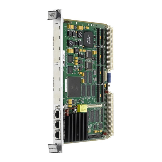
Motorola MVME5100 Manual
Single board computer
Hide thumbs
Also See for MVME5100:
- Programmer's reference manual (320 pages) ,
- Installation & use manual (107 pages) ,
- Specification sheet (5 pages)
Table of Contents
Advertisement
Quick Links
Advertisement
Table of Contents

Related Manuals for Motorola MVME5100


Summary of Contents for Motorola MVME5100
- Page 1 MVME5100 Single Board Computer Installation and Use V5100A/IH5 April 2006 Edition...
- Page 2 All rights reserved. Printed in the United States of America. Motorola and the Motorola logo are registered trademarks and AltiVec is a trademark of Motorola, Inc. PowerPC and the PowerPC logo are registered trademarks; and PowerPC 750 is a trademark of International Business Machines Corporation and are used by Motorola, Inc.
- Page 3 The safety precautions listed below represent warnings of certain dangers of which Motorola is aware. You, as the user of the product, should follow these warnings and all other safety precautions necessary for the safe operation of the equipment in your operating environment.
- Page 4 Flammability All Motorola PWBs (printed wiring boards) are manufactured with a flammability rating of 94V-0 by UL- recognized manufacturers. EMI Caution This equipment generates, uses and can radiate electromagnetic energy. It may cause or be susceptible to electromagnetic interference (EMI) if not installed and used with adequate EMI protection.
- Page 5 Motorola reserves the right to revise this document and to make changes from time to time in the content hereof without obligation of Motorola to notify any person of such revision or changes.
-
Page 7: Table Of Contents
MVME5100 ........ - Page 8 RAM500 Module Installation ............46 viii MVME5100 Installation and Use (V5100A/IH5)
- Page 9 Programming the MVME5100........
- Page 10 Related Specifications ............101 MVME5100 Installation and Use (V5100A/IH5)
- Page 11 Figure 1-2. MVME5100 Installation and Removal From a VMEbus Chassis ....8 Figure 1-3. Typical PMC Module Placement on an MVME5100 ......8 Figure 1-4.
- Page 13 Table 4-1. MVME5100 General Features ........
-
Page 15: About This Manual
MPC755 or MPC750. As of the printing date of this manual, the MVME5100 is available in the configurations shown below. These models are available with either VME Scanbe or IEEE 1101 compatible front panels. - Page 16 PMCSAN-010 with original VME Scanbe ejector handles RAM500-004 Stackable (top) 64MB ECC SDRAM mezzanine RAM500-006 Stackable (top) 256MB ECC SDRAM mezzanine RAM500-016 Stackable (bottom) 256MB ECC SDRAM mezzanine Contact your local Motorola sales representative for RoHS models of this board. MVME5100 Installation and Use (V5100A/IH5)
-
Page 17: Summary Of Changes
Chapter 2, Operation, provides a description of the operational functions of the MVME5100 including tips on applying power, a description of the switch settings, the status indicators, I/O connectors, and system power up information. -
Page 18: Comments And Suggestions
Firmware, provides an explanation of the debugger firmware, PPCBug, on the MVME5100. The chapter includes an overview of the firmware, a section on how to use PPCBug, a listing of the initialization steps, a brief explanation of the two main configuration commands CNFG and ENV, and a description of the standard configuration parameters. -
Page 19: Conventions Used In This Manual
In particular, assertion and assert refer to a signal that is active or true; negation and negate indicate a signal that is inactive or false. These terms are used independently of the voltage level (high or low) that they represent. Data and address sizes are defined as follows: MVME5100 Installation and Use (V5100A/IH5) - Page 20 16 bits, numbered 0 through 15, with bit 0 being the least significant. Word 32 bits, numbered 0 through 31, with bit 0 being the least significant. Double word 64 bits, numbered 0 through 63, with bit 0 being the least significant. MVME5100 Installation and Use (V5100A/IH5)
-
Page 21: Hardware Preparation And Installation
Overview and Equipment Requirements The MVME5100 interfaces to a VMEbus system via its P1 and P2 connectors and contains two IEEE 1386.1 PCI Mezzanine Card (PMC) Slots. The PMC Slots are 64-bit and support both front and rear I/O. -
Page 22: Unpacking Instructions
If the shipping carton(s) is/are damaged upon receipt, request that the carrier's agent be present during the unpacking and inspection of the equipment. Motorola strongly recommends that you use an antistatic wrist strap and a Use ESD conductive foam pad when installing or upgrading a system. -
Page 23: Preparation
A software readable header/ switch register (S1) is available on the MVME5100. This switch is not defined by the hardware and it is shipped in the OFF position, as are all the switches on this board. -
Page 24: Jumper Settings
For example, if you are using an IPMC761/MVME761 or IPMC712/MVME712 combination in conjunction with the MVME5100, you must reset the jumpers for the SBC mode (jumpers J4, J6, J10, J17 and J20). These are factory configured for the PMC mode. -
Page 25: Pmc/Sbc (761/Ipmc) Mode Selection
(PMC mode), or to the P2 connector via J4 (SBC mode). The other two headers (J6 and J20) ensure proper routing of +/- 12V signal routing. The MVME5100 is set at the factory for front panel I/O: PMC mode (see Table 1-1). The SBC mode should only be selected when using one of the IPMC-7xx modules in conjunction with the corresponding MVME7xx transition module. -
Page 26: Installation
1 Hardware Preparation and Installation Multiple MVME5100 boards may be installed in a single VME chassis; however, each must have a unique VMEbus address. Other MPUs on the VMEbus can interrupt, disable, communicate with, and determine the operational status of the processor(s). -
Page 27: Pmc Modules
1 Hardware Preparation and Installation PMC Modules PMC modules mount on top of the MVME5100. Perform the following steps to install a PMC module on your MVME5100. Dangerous voltages, capable of causing death, are present in this equipment. Use extreme caution when handling, testing and adjusting. -
Page 28: Primary Pmcspan
Figure 1-3. Typical PMC Module Placement on an MVME5100 Primary PMCspan To install a PMCspan-002 PCI expansion module on your MVME5100, perform the following steps while referring to the figure on the next page: Dangerous voltages, capable of causing death, are present in this equipment. -
Page 29: Figure 1-4. Pmcspan-002 Installation On An Mvme5100
MVME5100. – Thread the locking nuts into the standoff tips and tighten. 5. Place the PMCspan on top of the MVME5100. Align the mounting holes in each corner to the standoffs and align PMCspan connector P4 with MVME5100 connector J25. -
Page 30: Secondary Pmcspan
1 Hardware Preparation and Installation 6. Gently press the PMCspan and MVME5100 together and verify that P4 is fully seated in J25. 7. Insert four short screws (Phillips type) through the holes at the corners of the PMCspan and into the standoffs on the MVME5100. Tighten screws securely. -
Page 31: Mvme5100
AC cord or DC power lines from the system. Remove chassis or system cover(s) as necessary for access to the VME module. 3. If the Primary PMC Carrier Module and MVME5100 assembly is already installed in the VME chassis, carefully remove it as shown in... - Page 32 P1 and P2 connectors on the chassis backplane. Do not damage or bend connector pins. 5. Secure the MVME5100 (and PMCspans if used) in the chassis with the screws in the top and bottom of its front panel and verify proper contact with the transverse mounting rails to minimize RF emissions.
-
Page 33: Operation
Operation Introduction This chapter provides operating instructions for the MVME5100 Single Board Computer. It includes necessary information about powering up the system along with the functionality of the switches, status indicators and I/O ports on the front panels of the board. -
Page 34: Status Indicators
For additional information on pin assignments, refer to Chapter 6, Pin Assignments. port may be used for connecting a terminal to the MVME5100 to serve as the DEBUG firmware console for the factory installed debugger, PPCBug. The port is configured as follows:... -
Page 35: System Powerup
Initialization Process The MPU, hardware and firmware initialization process is performed by the PPCBug firmware upon system powerup or system reset. The firmware initializes the devices on the MVME5100 in preparation for booting an operating system. The firmware is shipped from the factory with an appropriate set of defaults. Depending on your system and specific application, there may or may not be a need to modify the firmware configuration before you boot the operating system. -
Page 37: Ppcbug Firmware
The PPCBug firmware is the layer of software just above the hardware. The firmware provides the proper initialization for the devices on the MVME5100 upon powerup or reset. This chapter describes the basics of the PPCBug and its architecture. It also describes the monitor (interactive command portion of the firmware), and provides information on using the PPCBug debugger and the special commands. -
Page 38: Implementation And Memory Requirements
After the debugger executes the command, the prompt reappears. However, depending on what the user program does, if the command causes execution of a user target code (that is, GO), then control may or may not return to the debugger. MVME5100 Installation and Use (V5100A/IH5) -
Page 39: Hardware And Firmware Initialization
The debugger performs the hardware and firmware initialization process. This process occurs each time the MVME5100 is reset or powered up. The steps listed below are a high-level outline; be aware that not all of the detailed steps are listed. -
Page 40: Default Settings
Use this command to display and configure the Board Information Block, which is resident within the NVRAM. This data block contains various elements detailing specific operational parameters of the MVME5100. The structure for the board is shown in the following example: Board (PWA) Serial Number... -
Page 41: Env - Set Environment
Refer to the PPCBug Firmware Package User's Manual for a description of the use of ENV. Additional information on registers in the Universe ASIC that affect these parameters is contained in your MVME5100 Programmer’s Reference Guide, listed in Appendix D, Related Documentation. - Page 42 Do not display the field service menu. (Default) Remote Start Method Switch [G/M/B/N] = B? The Remote Start Method Switch is used when the MVME5100 is cross-loaded from another VME-based CPU in order to start execution of the cross-loaded program.
- Page 43 (GEV). Do not give boot priority to devices listed in the fw-boot-path GEV. (Default) Note When enabled, the GEV boot takes priority over all other boots, including Autoboot and Network Boot. MVME5100 Installation and Use (V5100A/IH5)
- Page 44 “bootable” partition. That is then the partition that will be booted. Other acceptable values are 1, 2, 3 or 4. In these four cases, the partition specified will be booted without searching. MVME5100 Installation and Use (V5100A/IH5)
- Page 45 The last location tested when PPCBug searches for a ROMboot module. (Default = 0xFFFFFFFC) Network Auto Boot Enable [Y/N] = N? The Network Auto Boot (NETboot) function is enabled. The NETboot function is disabled. (Default) MVME5100 Installation and Use (V5100A/IH5)
- Page 46 NVRAM. Memory Size Enable [Y/N] = Y? Memory will be sized for SelfTest diagnostics. (Default) Memory will not be sized for SelfTest diagnostics. Memory Size Starting Address = 00000000? The default Starting Address is 0x00000000. MVME5100 Installation and Use (V5100A/IH5)
-
Page 47: Led/Serial Startup Diagnostic Codes
Serial Startup Code Master Enable [Y/N]=N? Should the debugger fail to come up to a prompt, the last code displayed will indicate how far the initialization sequence had progressed before stalling. Serial Startup Code LF Enable [Y/N]=N? MVME5100 Installation and Use (V5100A/IH5) -
Page 48: Configuring The Vmebus Interface
Documentation. Configuring the VMEbus Interface ENV asks the following series of questions to set up the VMEbus interface for the MVME5100. To perform this configuration, you should have a working knowledge of the Universe ASIC as described in your MVME5100 Programmer’s Reference Guide. Also, refer to the Tundra... - Page 49 The configured value is written into the VSI2_CTL register of the Universe chip. VMEbus Slave Image 2 Base Address Register = 00000000? The configured value is written into the VSI2_BS register of the Universe chip. MVME5100 Installation and Use (V5100A/IH5)
- Page 50 During this delay, you may press any key to prevent the execution of the startup command buffer. The default value of this parameter causes a startup delay of 5 seconds. Firmware Command Buffer: MVME5100 Installation and Use (V5100A/IH5)
-
Page 51: Firmware Command Buffer
Block of Memory Move Block of Memory Search Breakpoint Insert Block of Memory Verify CACHE Modify Cache State Concurrent Mode CNFG Configure Board Information Block Checksum a Block of data CSAR PCI Configuration Space READ Access MVME5100 Installation and Use (V5100A/IH5) - Page 52 Idle Master MPU I/O Control for Disk I/O Inquiry I/O Physical to Disk I/O “Teach” for Configuring Disk Controller Idle MPU Register Display Idle MPU Register Modify Idle MPU Register Set Load S-Records from Host MVME5100 Installation and Use (V5100A/IH5)
- Page 53 No Concurrent Mode NOMA Macro Delete NOMAL Disable Macro Expansion Listing NOPA Printer Detach NOPF Port Detach NORB No ROM Boot NOSYM Detach Symbol Table NPING Network Ping Offset Registers Display/Modify Printer Attach PBOOT Bootstrap Operating System MVME5100 Installation and Use (V5100A/IH5)
- Page 54 Flash memory is available to you, keep in mind that reprogramming any portion of Flash memory will erase everything currently contained in Flash, including the PPCBug debugger, if the target address addresses the bank in which it resides. MVME5100 Installation and Use (V5100A/IH5)
-
Page 55: Diagnostics
PPCBug’s diagnostic test groups are listed in Table 3-2. Note that not all tests are performed on the MVME5100. Using the HE command, you can list the diagnostic routines available in each test group. Refer to the PPCBug Diagnostics Manual, listed in Appendix D, Related... - Page 56 Refer to the documentation on a particular diagnostic for the correct mode. 3. Test Sets marked with an asterisk (*) are not available on the MVME5100 (unless an IPMC712 or IPMC761 is mounted). The ISABRDGE test is only performed if an IPMC761 is mounted on the MVME5100.
-
Page 57: Functional Description
The MVME5100’s advanced PowerPlus II Architecture supports full PCI throughput of 264MB without starving the CPU of its memory. Additional features of the MVME5100 include dual Ethernet ports, dual serial ports and up to 17MB of Flash. -
Page 58: Features Descriptions
(0° to 55° C) and industrial grade (–20° to 71° C) temperatures. The MVME5100 has two Input/Output (I/O) modes of operation: PMC and SBC (also called 761 mode or IPMC mode). In PMC mode, it is fully backwards compatible with previous generation dual PMC products such as the MVME2300 and MVME2400. -
Page 59: Processor
VME P1 Figure 4-1. MVME5100 Block Diagram Processor The MVME5100 incorporates a BGA foot print that supports both the MCP7410 and the MCP75x processors. The maximum external processor bus speed is 100 MHz. Note The MCP7410 is configured to operate only with the PowerPC 60xbus interface. -
Page 60: System Memory Controller And Pci Host Bridge
Motorola qualified Flash device used on this product) is a top-boot device, and as such, the write protected area is in the upper 16KB of each device. And, since Motorola is using 4 devices for the soldered Flash bank, the write protected region corresponds to the upper 64KB of the soldered Flash memory map. -
Page 61: Ecc Sdram Memory
P2 Input/Output (I/O) Modes The MVME5100 has two P2 I/O modes (SBC and PMC) that are user- configurable with jumpers on the board (J6 and J20). The jumpers route the on-board Ethernet port 2 to row C of the P2 connector. -
Page 62: Vmebus Interface
Timers Timers and counters on the MVME5100 are provided by the board’s hardware (Hawk ASIC). There are four 32-bit timers on the board that may be used for system timing or to generate periodic interrupts. -
Page 63: Ram500 Memory Expansion Module
RAM500 Memory Expansion Module Overview The RAM500 memory expansion module can be used on the MVME5100 as an option for additional memory capability. Each expansion module is a single bank of SDRAM with up to 256MB of available ECC memory. Currently, two expansion modules can be used in tandum to produce an additional expanded memory capability of 512MB. -
Page 64: Ram500 Description
The RAM500 is a memory expansion module that is used on the MVME5100 Single Board Computer, and will be used on other Motorola products in the future. The RAM500 is based on a single memory mezzanine board design with the flexibility of being populated with different sized SDRAM components and SPD options to provide a variety of memory configurations. -
Page 65: Srom
$AA. The second RAM500 attached to the host board has its SPD addressable at $AC. This dynamic address relocation of the RAM500 SPD shall be done using the bottom- side connector signal A1_SPD and A0_SPD. MVME5100 Installation and Use (V5100A/IH5) -
Page 66: Host Clock Logic
AC cord or DC power lines from the system. Remove the chassis or system cover(s) as necessary for access to the CompactPCI boards. 3. Carefully remove the MVME5100 from its VME card slot and lay it flat, with connectors P1 and P2 facing you. -
Page 67: Ram500 Connectors
8. Turn the entire assembly over, and fasten the three nuts provided to the standoff posts on the bottom of the MVME5100 host board. 9. Reinstall the MVME5100 assembly in its proper card slot. Be sure the host board is well seated in the backplane connectors. Do not damage or bend connector pins. - Page 68 DQ37 DQ38 DQ39 +3.3V +3.3V DQ40 DQ41 DQ42 DQ43 DQ44 DQ45 DQ46 DQ47 GND* GND* DQ48 DQ49 DQ50 DQ51 DQ52 DQ53 +3.3V +3.3V DQ54 DQ55 DQ56 DQ57 DQ58 DQ59 DQ60 DQ61 GND* GND* DQ62 DQ63 MVME5100 Installation and Use (V5100A/IH5)
- Page 69 AMP that includes receptacles loaded with contacts for grounding circuits at 9 or 10 signal circuits. These ground contacts mate with grounding plates on both sides of the plug assemblies. MVME5100 Installation and Use (V5100A/IH5)
-
Page 70: Top Side Memory Expansion Connector (J1)
DQ17 DQ18 DQ19 DQ20 DQ21 DQ22 DQ23 +3.3V +3.3V DQ24 DQ25 DQ26 DQ27 DQ28 DQ29 DQ30 DQ31 GND* GND* DQ32 DQ33 DQ34 DQ35 DQ36 DQ37 DQ38 DQ39 +3.3V +3.3V DQ40 DQ41 DQ42 DQ43 DQ44 DQ45 MVME5100 Installation and Use (V5100A/IH5) - Page 71 DQ56 DQ57 DQ58 DQ59 DQ60 DQ61 GND* GND* DQ62 DQ63 CKD00 CKD01 CKD02 CKD03 CKD04 CKD05 +3.3V +3.3V CKD06 CKD07 GND* GND* +3.3V +3.3V CS_E0_L GND* CS_E1_L WE_L RAS_L GND* GND* CAS_L +3.3V +3.3V DQMB1 MVME5100 Installation and Use (V5100A/IH5)
-
Page 72: Ram500 Programming Issues
Computer Programmer’s Reference Guide. The register is accessed through the I C interface of the Hawk ASIC on the host board (MVME5100). The RAM500 SPD is software addressable by a unique address as follows: The first RAM500 attached to the host board has has an SPD address of $AA. -
Page 73: Pin Assignments
COM2 Interface Protection Jumper Settings The following table provides information about the jumper settings associated with th MVME5100 Single Board Computer. The table below provides a brief description of each jumper and the appropriate setting(s) for proper board operation. Jumper Description... -
Page 74: Connectors
This connetor is used to provide an interface to the IPMC761 module signals and is located near J11. The pin assignments for this connector are as follows: Table 6-1. IPMC761 Connector Pin Assignments Assignment I2CSCL I2CSDA DB8# DB9# DB10# +3.3V +3.3V DB11# DB12# DB13# MVME5100 Installation and Use (V5100A/IH5) -
Page 75: Memory Expansion Connector (J8) Pin Assignments
Table 6-2. Memory Expansion Connector Pin Assignments Assignment DQ00 DQ01 DQ02 DQ03 DQ04 DQ05 DQ06 DQ07 +3.3V +3.3V DQ08 DQ09 DQ10 DQ11 DQ12 DQ13 DQ14 DQ15 DQ16 DQ17 DQ18 DQ19 DQ20 DQ21 MVME5100 Installation and Use (V5100A/IH5) - Page 76 DQ41 DQ42 DQ43 DQ44 DQ45 DQ46 DQ47 DQ48 DQ49 DQ50 DQ51 DQ52 DQ53 +3.3V +3.3V DQ54 DQ55 DQ56 DQ57 DQ58 DQ59 DQ60 DQ61 DQ62 DQ63 CKD00 CKD01 CKD02 CKD03 CKD04 CKD05 +3.3V +3.3V CKD06 CKD07 MVME5100 Installation and Use (V5100A/IH5)
-
Page 77: Pci Expansion Connector (J25) Pin Assignments
This may cause the clock generation logic to set the local bus frequency to 83.33 MHz if necessary. PCI Expansion Connector (J25) Pin Assignments This connector is used to provide PCI/PMC expansion capability. The pin assignments for this connector are as follows: MVME5100 Installation and Use (V5100A/IH5) -
Page 78: Table 6-3. Pci Expansion Connector Pin Assignments
Table 6-3. PCI Expansion Connector Pin Assignments Assignment +3.3V +3.3V PCICLK PMCINTA# PMCINTB# PURST# PMCINTC# HRESET# PMCINTD# TRST# PCIXP# PCIXGNT# PCIXREQ# +12V -12V PERR# SERR# LOCK# SDONE DEVSEL# SBO# TRDY# IRDY# STOP# FRAME# ACK64# Reserved REQ64# Reserved MVME5100 Installation and Use (V5100A/IH5) - Page 79 Table 6-3. PCI Expansion Connector Pin Assignments (continued) Assignment PCIRST# C/BE1# C/BE0# C/BE3# C/BE2# AD11 AD10 AD13 AD12 AD15 AD14 AD17 AD16 AD19 AD18 AD21 AD20 AD23 AD22 AD25 AD24 AD27 AD26 AD29 AD28 AD31 AD30 MVME5100 Installation and Use (V5100A/IH5)
-
Page 80: Pci Mezzanine Card (Pmc) Connectors
These connectors provide 32/64-bit PCI interfaces and P2 I/O for two optional add-on PCI Mezzanine Cards (PMC). The pin assignments for these connectors are as follows. Table 6-4. PMC Slot 1 Connector (J11) Pin Assignments Assignment -12V INTA# INTB# INTC# PMCPRSNT1# INTD# Not Used Not Used MVME5100 Installation and Use (V5100A/IH5) - Page 81 +5V (Vio) AD31 AD28 AD27 AD25 C/BE3# AD22 AD21 AD19 +5V (Vio) AD17 FRAME# IRDY# DEVSEL# LOCK# SDONE# SBO# +5V (Vio) AD15 AD12 AD11 AD09 C/BE0# AD06 AD05 AD04 +5V (Vio) AD03 AD02 AD01 AD00 REQ64# MVME5100 Installation and Use (V5100A/IH5)
-
Page 82: Table 6-5. Pmc Slot 1 Connector (J12) Pin Assignments
AD18 AD16 C/BE2# Not Used TDRY# +3.3V STOP# PERR# +3.3V SERR# C/BE1# AD14 AD13 AD10 AD08 +3.3V AD07 Not Used +3.3V Not Used Not Used Not Used Not Used Not Used ACK64# +3.3V Not Used MVME5100 Installation and Use (V5100A/IH5) - Page 83 +5V (Vio) AD56 AD55 AD54 AD53 AD52 AD51 AD50 AD49 AD48 AD47 AD46 AD45 +5V (Vio) AD44 AD43 AD42 AD41 AD40 AD39 AD38 AD37 AD36 AD35 AD34 AD33 +5V (Vio) AD32 Reserved Reserved Reserved Reserved MVME5100 Installation and Use (V5100A/IH5)
-
Page 84: Table 6-6. Pmc Slot 1 Connector (J14) Pin Assignments
PMC1_47 (P2-C24) PMC1_48 (P2-A24) PMC1_49 (P2-C25) PMC1_50 (P2-A25) PMC1_51 (P2-C26) PMC1_52 (P2-A26) PMC1_53 (P2-C27) PMC1_54 (P2-A27) PMC1_55 (P2-C28) PMC1_56 (P2-A28) PMC1_57 (P2-C29) PMC1_58 (P2-A29) PMC1_59 (P2-C30) PMC1_60 (P2-A30) PMC1_61 (P2-C31) PMC1_62 (P2-A31) PMC1_63 (P2-C32) PMC1_64 (P2-A32) MVME5100 Installation and Use (V5100A/IH5) - Page 85 AD27 AD25 C/BE3# AD22 AD21 AD19 +5V (Vio) AD17 FRAME# IRDY# DEVSEL# LOCK# SDONE# SBO# +5V (Vio) AD15 AD12 AD11 AD09 C/BE0# AD06 AD05 AD04 +5V (Vio) AD03 AD02 AD01 AD00 REQ64# Assignment +12V TRST# MVME5100 Installation and Use (V5100A/IH5)
- Page 86 +3.3V AD07 Not Used +3.3V Not Used Not Used Not Used Not Used Not Used ACK64# +3.3V Not Used Assignment Reserved C/BE7# C/BE6# C/BE5# C/BE4# +5V (Vio) PAR64 AD63 AD62 AD61 AD60 AD59 AD58 AD57 MVME5100 Installation and Use (V5100A/IH5)
- Page 87 PMC2_17 (P2-Z11) PMC2_18 (P2-D12) PMC2_19 (P2-D13) PMC2_20 (P2-Z13) PMC2_21 (P2-D14) PMC2_22 (P2-D15) PMC2_23 (P2-Z15) PMC2_24 (P2-D16) PMC2_25 (P2-D17) PMC2_26 (P2-Z17) PMC2_27 (P2-D18) PMC2_28 (P2-D19) PMC2_29 (P2-Z19) PMC2_30 (P2-D20) PMC2_31 (P2-D21) PMC2_32 (P2-Z21) PMC2_33 (P2-D22 PMC2_34 (P2-D23) MVME5100 Installation and Use (V5100A/IH5)
-
Page 88: Vmebus Connectors P1 & P2 Pin Assignments (Pmc Mode)
The pin assignments for the connector are specified by the IEEE P1014-1987 VMEbus Specification and the VME64 Extension Standard. Row B of connector P2 provides power to the MVME5100, and to the upper eight VMEbus address lines, and additional 16 VMEbus data lines. Rows A, C, Z and D provide power and interface signals to the MVME762 transition module. -
Page 89: Vmebus P1 & P2 Connector Pin Assignments (Sbc Mode)
The pin assignments for the connector are specified by the IEEE P1014-1987 VMEbus Specification and the VME64 Extension Standard. Row B of connector P2 provides power to the MVME5100 and to the upper 8 VMEbus address lines and additional 16 VMEbus data lines. - Page 90 MCLK Note Rows A and C and Z’s (Z1, 3, 5 , 7, 9, 11, 13, 15 and 17) functionality is provided by the IPMC761 in slot 1 and the MVME5100 Ethernet port 2. Row Z Row A Row B...
-
Page 91: 10 Baset/100 Basetx Connector Pin Assignments
The board’s dual 10 BaseT/100 BaseTx RJ45 connectors (J9 and J18) are located on the front plate. The connections provide two LAN connections (LAN1-J18 and LAN2-J9). The pin assignments for these connectors are as follows: Assignment MVME5100 Installation and Use (V5100A/IH5) -
Page 92: Com1 And Com2 Connector Pin Assignments
A standard RJ45 connector located on the front panel and a 9-pin header located near the bottom edge of the MVME5100 provides the interface to the serial debug ports. The RJ45 connector is for COM1 and the 9-pin header is for COM2. -
Page 93: Programming The Mvme5100
For programming information about the PMCs, refer to the applicable user’s manual furnished with the PMCs. Memory Maps There are multiple buses on the MVME5100 and each bus domain has its own view of the memory map. The following sections describe the MVME5100 memory organization from the following three points of view:... -
Page 94: Default Processor Memory Map
For an example of the CHRP memory map, refer to the following table. For detailed processor memory maps, including suggested CHRP- and PREP-compatible memory maps, refer to the MVME5100-Series Single Board Computer Programmer’s Reference Guide. MVME5100 Installation and Use (V5100A/IH5) -
Page 95: Processor Memory Map
3. The first 1MB of ROM/FLASH Bank A appears at this range after a reset if the rom_b_rv control bit is cleared. If the rom_b_rv control bit is set, this address maps to ROM/FLASH Bank B. MVME5100 Installation and Use (V5100A/IH5) -
Page 96: Pci Memory Map
0000 0000 PCI Memory Map Following a reset, the Hawk ASIC disables all PCI slave map decoders. The MVME5100 is fully capable of supporting both PREP and CHRP PCI Memory Maps with RAM size limited to 2GB. VME Memory Map The MVME5100 is fully capable of supporting both the PREP and the CHRP VME Memory Maps examples with RAM size limited to 2GB. -
Page 97: Programming Considerations
VMEbus-to-local-bus interface. The address translation capabilities of the Universe enable the processor to access any range of addresses on the VMEbus. Recommendations for VMEbus mapping, including suggested CHRP- and PREP-compatible memory maps, can be found in the MVME5100-Series Single Board Computer Programmer’s Reference Guide. Figure 7-1 shows the overall mapping approach from the standpoint of a VMEbus master. -
Page 98: Figure 7-1. Vmebus Master Mapping
2. Programmable mapping performed via PCI Slave images in Universe ASIC. 3. Programmable mapping performed via Special Slave image (SLSI) in Universe ASIC. Figure 7-1. VMEbus Master Mapping The arbitration assignments for the MVME5100 are shown in Table 7-4. Table 7-4. PCI Arbitration Assignments... -
Page 99: Interrupt Handling
Interrupt Handling The Hawk ASIC, which controls the PHB (PCI Host Bridge) and the MPU/local bus interface functions on the MVME5100, performs interrupt handling as well. Sources of interrupts may be any of the following: The Hawk ASIC itself (timer interrupts, transfer error interrupts or memory error... -
Page 100: Dma Channels
SERR_& PERR_ PCI Interrupts ISA Interrupts 11559.00 9609 Figure 7-2. MVME5100 Interrupt Architecture The MVME5100 routes the interrupts from the PMCs and PCI expansion slots as follows: PMC Slot 1 PMC Slot 2 PCIX Slot INTA# INTB# INTC# INTD# INTA# INTB# INTC# INTD#... -
Page 101: Sources Of Reset
System Software reset, Local Software Reset and VME CSR Reset functions. Note On the MVME5100, Watchdog Timer 2 is a source of reset only if component R206 is installed on the board. Consult your local Embedded Communications Computing Group (ECCG) sales representative if this feature needs to be enabled. -
Page 102: Endian Issues
7 Programming the MVME5100 Endian Issues The MVME5100 supports both little-endian (e.g., Windows NT) and big-endian (e.g., AIX) software. The PowerPC processor and the VMEbus are inherently big-endian, while the PCI bus is inherently little-endian. The following sections summarize how the MVME5100 handles software and hardware differences in big- and little-endian operations. -
Page 103: Vmebus Domain
In little-endian mode, however, software must take the byte-swapping effect of the Universe ASIC and the address reverse-rearranging effect of the PHB into account. For further details on endian considerations, refer to the MVME5100-Series Single Board Computer Programmer’s Reference Guide. -
Page 105: Specifications
Specifications This appendix lists general specifications and power characteristics for the MVME5100 Single Board Computer. It also provides information on cooling requirements. A complete functional description of the MVME5100 Single Board Computer appears in Chapter 4, Functional Description. Specifications for the optional PMC modules can be found in the documentation for those modules. -
Page 106: Power Requirements
A Specifications Power Requirements Power requirements for the MVME5100 Single Board Computer depend on the configuration of the board. The table below lists the typical and maximum power consumption of the board using an MVME761 Transition Module. Table A-2. Power Consumption... -
Page 107: Troubleshooting
Troubleshooting Solving Startup Problems In the event of difficulty with your MVME5100, perform the simple troubleshooting steps listed in the table below before calling for help or sending the board back for repair. Some of the procedures will return the board to the factory debugger environment. It is important to note that the Board was tested under these conditions before it left the factory. - Page 108 The date and time will be autoboot. incorrectly. displayed. B. There may be CAUTION: Performing the next step (env;d) some fault in the will change some parameters that may affect board hardware. your system’s operation. MVME5100 Installation and Use (V5100A/IH5)
- Page 109 V. V. The debugger A. No apparent No further troubleshooting steps are required. is in system problems — mode; the board troubleshooting autoboots, or the is done. board has passed self tests. MVME5100 Installation and Use (V5100A/IH5)
- Page 110 2. Phone 1-800-222-5640. listed above; or the on-board cannot be debugging and corrected using diagnostic the steps given. firmware. TROUBLESHOOTING PROCEDURE COMPLETE MVME5100 Installation and Use (V5100A/IH5)
-
Page 111: Thermal Analysis
The preferred temperature measurement location for a component may be: junction - refers to the temperature measured by an on-chip thermal device case - refers to the temperature at the top, center surface of the component MVME5100 Installation and Use (V5100A/IH5) -
Page 112: Table C-1. Thermally Significant Components On The Mvme5100 Single Board Computer
C Thermal Analysis air - refers to the ambient temperature near the component Table C-1. Thermally Significant Components on the MVME5100 Single Board Computer Reference Generic Description Maximum Measurement Designator? Allowable Location Component Temperature (degrees C) Hawk ASIC Junction ECC DRAM (NEC D4564841G5) -
Page 113: Figure C-1. Thermally Significant Components On The Mvme5100 Sbc - Primary Side
C Thermal Analysis Note An MVME5100 Single Board Computer and an IPMC761 I/O board was tested in a Motorola lab environment, and it was verified that the reliability of the components would not be compromised when operating in a maximum ambient temperature of 55 degrees C, if the required airflow of 400 LFM is provided. -
Page 114: Component Temperature Measurement
Table C-1. Preparation We recommend 40-gage thermocouples for all thermal measurements. Larger gage thermocouples can wick heat away from the components and disturb air flowing past the board. MVME5100 Installation and Use (V5100A/IH5) -
Page 115: Measuring Junction Temperature
Measuring Junction Temperature Some components have an on-chip thermal measuring device such as a thermal diode. For instructions on measuring temperatures using the on-board device, refer to the MVME5100 component manufacturer’s documentation listed in Appendix D, Related Documentation. -
Page 116: Measuring Local Air Temperature
Measure local component ambient temperature by placing the thermocouple downstream of the component. This method is conservative since it includes heating of the air by the component. Figure C-4 shows one method of mounting the thermocouple. MVME5100 Installation and Use (V5100A/IH5) -
Page 117: Figure C-4. Measuring Local Air Temperature
C Thermal Analysis Tape thermocouple wire to top of component Thermocouple junction Air flow Figure C-4. Measuring Local Air Temperature MVME5100 Installation and Use (V5100A/IH5) -
Page 119: Related Documentation
Related Documentation Embedded Communications Computing Documents The Motorola publications listed below are referenced in this manual. You can obtain paper or electronic copies of Embedded Communications Computing publications by: Contacting your local Motorola sales office Visiting Embedded Communications Computing World Wide Web literature site, http://www.motorola.com/computer/literature... -
Page 120: Manufacturers' Documents
M48T37V CMOS 32Kx8 Timekeeper SRAM Data M48T37V Sheet SGS Thomson Microelectronics tap//.us.st.com 2-Wire Serial CMOS EEPROM Data Sheet AT24C04 Atmel Corporation San Jose, CA Intel GD82559ER Fast Ethernet PCI Controller 714682-001 Datasheet Rev. 1.0 Intel Corporation March 1999 MVME5100 Installation and Use (V5100A/IH5) -
Page 121: Related Specifications
Common Mezzanine Card Specification P1386 IEEE Standards Department Draft 2.0 445 Hoes Lane, P.O Box 1331 Piscataway, NJ 08855-1331 PCI Mezzanine Card Specification P1386.1 Draft 2.0 IEEE Standards Department 445 Hoes Lane, P.O Box 1331 Piscataway, NJ 08855-1331 MVME5100 Installation and Use (V5100A/IH5) - Page 123 Network Auto Boot Controller comments, sending xviii NVRAM Bootlist component temperature measurement Primary SCSI Bus Negotiations configurable items, MVME5100 base board Primary SCSI Data Bus Width configurations ROM Boot Enable MVME5100 SCSI bus reset on debugger startup configure...
- Page 124 Memory Expansion IACK and BG signals memory map IDSEL routing CHRP initialization PCI local bus performed by PPCBug processor (default) initialization process memory maps as performed by firmware MVME5100 Input/Output Interface VMEbus installation memory size MVME5100 Installation and Use (V5100A/IH5)
- Page 125 J1/P1, RAM500 programming mvme5100 slot 1 arbiter description slot 2 arbiter PMC Carrier Board Placement on MVME5100 PMC Interface (Slot 1) Negate VMEbus SYSFAIL* Always PMC Interface (Slot 2) NETboot enable PMC mode Network Auto Boot Controller jumper settings...
- Page 126 VMEbus Interface switch VMEbus interface abort reset switches Winbond PCI/ISA bus bridge controller switches, MVME5100 front panel Winbond W83C553 SYSFAIL* as PCI arbiter support MVME5100 Installation and Use (V5100A/IH5)
- Page 127 MVME5100 Single Board Computer Installation and Use...
Need help?
Do you have a question about the MVME5100 and is the answer not in the manual?
Questions and answers