Sign In
Upload
Manuals
Brands
Artesyn Manuals
Motherboard
MVME2500ET-0171
Artesyn MVME2500ET-0171 Manuals
Manuals and User Guides for Artesyn MVME2500ET-0171. We have
1
Artesyn MVME2500ET-0171 manual available for free PDF download: Installation And Use Manual
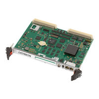
Artesyn MVME2500ET-0171 Installation And Use Manual (152 pages)
Brand:
Artesyn
| Category:
Motherboard
| Size: 9 MB
Table of Contents
Table of Contents
3
List of Figures
12
About this Manual
13
Summary of Changes
17
Safety Notes
19
Sicherheitshinweise
23
1 Introduction
29
Overview
29
Standard Compliances
31
Table 1-1 Board Standard Compliances
31
Figure 1-1 MVME2500 Declaration of Conformity
32
Mechanical Data
33
Ordering Information
33
Table 1-3 Available Board Variants
33
Table 1-4 Available Board Accessories
34
Product Identification
35
Figure 1-2 Serial Number Location
35
2 Hardware Preparation and Installation
37
Overview
37
Unpacking and Inspecting the Board
38
Requirements
39
Environmental Requirements
39
Table 2-1 Environmental Requirements
39
Power Requirements
40
Table 2-2 Power Requirements
41
Equipment Requirements
42
Configuring the Board
42
Installing Accessories
43
Rear Transition Module
43
PMC/XMC Support
45
Installing and Removing the Board
46
Completing the Installation
48
3 Controls, Leds, and Connectors
49
Board Layout
49
Figure 3-1 Component Layout
49
Front Panel
50
Figure 3-2 Front Panel Leds, Connectors and Switches
50
Reset Switch
51
Leds
51
Front Panel Leds
51
Table 3-1 Front Panel Leds
52
On-Board Leds
53
Connectors
53
Table 3-2 On-Board Leds Status
53
Front Panel Connectors
54
RJ45 with Integrated Magnetics (J1)
54
Table 3-3 Front Panel Tri-Speed Ethernet Connector (J1)
54
Front Panel Serial Port (J4)
55
Table 3-4 Front Panel Serial Port (J4)
55
Table 3-6 Vmebus P1 Connector
56
USB Connector (J5)
56
Vmebus P1 Connector
56
Table 3-7 Vmebus P2 Connector
58
Vmebus P2 Connector
58
On-Board Connectors
59
Flash Program Connector (P7)
59
Table 3-8 Flash Programming Header (P7)
59
SATA Connector (J3)
60
Table 3-9 Custom SATA Connector (J3)
60
Figure
61
PMC Connectors
61
Table 3-11 PMC J12 Connector
62
Table 3-12 PMC J13 Connector
64
Table 3-13 PMC J14 Connector
65
JTAG Connector (P6)
66
COP Connector (P50)
68
SD Connector (J2)
69
Table 3-17 XMC Connector (XJ2) Pinout
69
XMC Connector (XJ2)
69
Miscellaneous P2020 Debug Connectors
70
Table 3-18 P20X0 Debug Header
70
Switches
71
Geographical Address Switch (S1)
71
Table 3-19 Geographical Address Switch
72
Figure 3-5 Geographical Address Switch
72
SMT Configuration Switch (S2)
73
Table 3-10 Table
73
Table 3-20 Geographical Address Switch Settings
73
Figure 3-6 SMT Configuration Switch Position
73
4 Functional Description
77
Block Diagram
77
Chipset
78
E500 Processor Core
78
Integrated Memory Controller
79
PCI Express Interface
79
Local Bus Controller (LBC)
80
Secure Digital Hub Controller (SDHC)
80
I2C Interface
80
USB Interface
80
Duart
80
DMA Controller
81
Enhanced Three-Speed Ethernet Controller (Etsec)
81
General Purpose I/O (GPIO)
81
Security Engine (SEC) 3.1
81
Common On-Chip Processor (COP)
82
P20X0 Hardware Configuration Pins
82
System Memory
82
Timers
82
Real Time Clock
82
Internal Timer
83
Watchdog Timer
83
FPGA Tick Timer
83
Ethernet Interfaces
83
SPI Bus Interface
84
SPI Flash Memory
84
SPI Flash Programming
84
Firmware Redundancy
85
Figure 4-2 SPI Device Multiplexing Logic
86
Crisis Recovery
87
Front UART Control
87
Rear UART Control
88
PMC/XMC Sites
88
PMC Add-On Card
89
XMC Add-On Card
89
SATA Interface
90
VME Support
90
Tsi148 VME Controller
90
Usb
90
I2C Devices
91
Reset/Control FPGA
91
Power Management
91
On-Board Voltage Supply Requirement
92
Power up Sequencing Requirements
92
Table 4-1 Voltage Supply Requirement
92
Figure 4-3 Power up Sequence
93
Clock Structure
94
Reset Structure
94
Figure 4-4 Clock Distribution Diagram
94
Reset Sequence
95
Figure 4-5 Reset Sequence
96
Reset Sequence
96
Thermal Management
97
Real-Time Clock Battery
97
Debugging Support
97
Table 4-2 Thermal Interrupt Threshold
97
JTAG Chain and Board
98
POST Code Indicator
98
Table 4-3 POST Code Indicator on the LED
98
Custom Debugging
99
Rear Transition Module (RTM)
99
Table 4-4 Transition Module Features
99
5 Memory Maps and Registers
101
Overview
101
Memory Map
101
Table 5-1 Physical Address Map
101
Flash Memory Map
102
Linux Devices Memory Map
102
Table 5-3 Linux Devices Memory Map
102
Programmable Logic Device (PLD) Registers
104
PLD Revision Register
104
PLD Year Register
104
Table 5-4 PLD Revision Register
104
PLD Month Register
105
PLD Day Register
105
PLD Sequence Register
105
Table 5-6 PLD Month Register
105
Table 5-8 PLD Sequence Register
105
PLD Power Good Monitor Register
106
Table 5-9 PLD Power Good Monitor Register
106
PLD LED Control Register
107
Table 5-10 PLD LED Control Register
107
PLD PCI/PMC/XMC Monitor Register
108
Table 5-11 PLD PCI/PMC/XMC Monitor Register
108
PLD U-Boot and TSI Monitor Register
109
PLD Boot Bank Register
109
Table 5-12 PLD U-Boot and TSI Monitor Register
109
Table 5-13 PLD Boot Bank Register
109
PLD Write Protect and I2C Debug Register
110
Table 5-14 PLD Write Protect and I2C Debug Register
110
PLD Test Register 1
112
PLD Test Register 2
112
PLD GPIO2 Interrupt Register
113
Table 5-17 PLD GPIO2 Interrupt Register
113
PLD Shutdown and Reset Control and Reset Reason Register
114
Table 5-18 PLD Shutdown and Reset Control and Reset Reason Register
114
PLD Watchdog Timer Refresh Register
115
Table 5-19 PLD Watchdog Timer Refresh Register
115
PLD Watchdog Control Register
116
PLD Watchdog Timer Count Register
116
Table 5-20 PLD Watchdog Control Register
116
Table 5-21 PLD Watchdog Timer Count Register
116
External Timer Registers
117
Prescaler Register
117
Table 5-22 Prescaler Register
117
Control Registers
118
Compare High and Low Word Registers
119
Table 5-24 Compare High Word Registers
119
Table 5-25 Compare Low Word Registers
119
Counter High and Low Word Registers
120
Table 5-26 Counter High Word Registers
120
Table 5-27 Counter Low Word Registers
120
6 Boot System
121
Overview
121
Accessing U-Boot
121
Boot Options
122
Booting from a Network
122
Booting from an Optional SATA Drive
123
Booting from a USB Drive
123
Booting from an SD Card
124
Booting Vxworks through the Network
124
Using the Persistent Memory Feature
125
MVME2500 Specific U-Boot Commands
126
Table 6-1 MVME2500 Specific U-Boot Commands
126
Updating U-Boot
128
7 Programming Model
131
Overview
131
Reset Configuration
131
Table 7-1 por Configuration Settings
131
Interrupt Controller
135
Table 7-2 MVME2500 Interrupt List
135
I2C Bus Device Addressing
136
Ethernet PHY Address
136
Table 7-3 I2C Bus Device Addressing
136
Table 7-4 PHY Types and MII Management Bus Address
136
Other Software Considerations
137
Mram
137
Real Time Clock
137
Quad UART
138
LBC Timing Parameters
138
Table 7-5 LBC Timing Parameters
138
Clock Distribution
139
Table 7-6 Clock Distribution
139
System Clock
140
Local Bus Controller Clock Divisor
141
Real Time Clock Input
141
Replacing the Battery
143
Figure A-1 Battery Location
143
Table B-1 Artesyn Embedded Technologies - Embedded Computing Publications
147
Related Specifications
148
Table B-2 Manufacturers' Publications
148
B.2 Manufacturers' Documents
148
Related Documentation
149
Advertisement
Advertisement
Related Products
Artesyn MVME2500ET-0163
Artesyn MVME2500ET-0161
Artesyn MVME2500ET-0173
Artesyn MVME2500-ECC
Artesyn MVME2500-01080101E
Artesyn MVME2500-01080101S
Artesyn MVME2500-021CC
Artesyn MVME2500-0163
Artesyn MVME2500-0161
Artesyn MVME2500-02120201S
Artesyn Categories
Motherboard
Server
Single board computers
PCI Card
Control Unit
More Artesyn Manuals
Login
Sign In
OR
Sign in with Facebook
Sign in with Google
Upload manual
Upload from disk
Upload from URL