
Related Manuals for Altera Stratix V GX FPGA


Summary of Contents for Altera Stratix V GX FPGA
-
Page 1: Reference Manual
Stratix V GX FPGA Development Board Reference Manual 101 Innovation Drive San Jose, CA 95134 www.altera.com MNL-01063-1.6 Feedback Subscribe... - Page 2 © 2015 Altera Corporation. All rights reserved. ALTERA, ARRIA, CYCLONE, HARDCOPY, MAX, MEGACORE, NIOS, QUARTUS and STRATIX words and logos are trademarks of Altera Corporation and registered in the U.S. Patent and Trademark Office and in other countries. All other words and logos identified as trademarks or service marks are the property of their respective holders as described at www.altera.com/common/legal.html.
-
Page 3: Table Of Contents
Featured Device: Stratix V GX FPGA ........ - Page 4 How to Contact Altera ........
-
Page 5: Chapter 1. Overview
FPGA designs that interface with all components of the board. General Description The Stratix V GX FPGA development board provides a hardware platform for developing and prototyping high-performance and high-bandwidth application designs. The board provides a wide range of peripherals and memory interfaces to facilitate the development of Stratix V GX FPGA designs. -
Page 6: Board Component Blocks
1–2 Chapter 1: Overview Board Component Blocks Board Component Blocks The board features the following major component blocks: ■ Altera Stratix V FPGA (5SGXEA7K2F40C2N) in the 1517-pin FineLine BGA Package 622,000 LEs ■ 234,720 adaptive logic modules (ALMs) ■ 50-Mbits (Mb) embedded memory ■... - Page 7 ■ ■ System Monitoring Power—voltage, current, wattage ■ Temperature—FPGA die, local board ■ Mechanical ■ PCI Express short form factor ■ PCI Express chassis or bench-top operation ■ September 2015 Altera Corporation Stratix V GX FPGA Development Board Reference Manual...
-
Page 8: Development Board Block Diagram
1–4 Chapter 1: Overview Development Board Block Diagram Development Board Block Diagram Figure 1–1 shows the block diagram of the Stratix V GX FPGA Development Board. Figure 1–1. Stratix V GX FPGA Development Board Block Diagram DQS/Single-Ended LVDS/Single-Ended Micro-USB On-Board... -
Page 9: Board Components
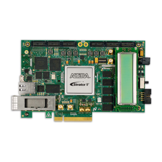
2. Board Components This chapter introduces all the important components on the Stratix V GX FPGA Development Board. Figure 2–1 illustrates major component locations and Table 2–1 provides a brief description of all features of the board. A complete set of schematics, a physical layout database, and GERBER files for the development board reside in the Stratix V GX FPGA development kit documents directory. -
Page 10: Chapter 2. Board Components
2–2 Chapter 2: Board Components Board Overview Board Overview This section provides an overview of the Stratix V GX FPGA development board, including an annotated board image and component descriptions. Figure 2–1 provides an overview of the development board features. - Page 11 Chapter 2: Board Components 2–3 Board Overview Table 2–1. Stratix V GX FPGA Development Board Components (Part 2 of 4) Board Reference Type Description Controls the PCI Express lane width by connecting prsnt pins PCI Express DIP switch together on the PCI Express edge connector. This switch is located at the back of the board.
- Page 12 2–4 Chapter 2: Board Components Board Overview Table 2–1. Stratix V GX FPGA Development Board Components (Part 3 of 4) Board Reference Type Description 50 M oscillator 50.000-MHz crystal oscillator for general purpose logic. Drives LVPECL-compatible clock inputs into the clock multiplexer...
-
Page 13: Featured Device: Stratix V Gx Fpga
LEs, lead free I/O Resources Table 2–4 lists the Stratix V GX FPGA device pin count and usage by function on the development board. Table 2–4. Stratix V GX FPGA Pin Count and Usage (Part 1 of 2) Function... -
Page 14: Max V Cpld System Controller
2–6 Chapter 2: Board Components MAX V CPLD System Controller Table 2–4. Stratix V GX FPGA Pin Count and Usage (Part 2 of 2) Function I/O Standard I/O Count Special Pins Flash 1.8-V CMOS — PCI Express ×8 2.5-V CMOS + XCVR... - Page 15 FPGA reset push button CPU_RESETn DIP - load factory image or user1 image from — 2.5-V FACTORY_LOAD flash at power-up On-Board USB-Blaster II request to send — 1.8-V FACTORY_REQUEST FACTORY command September 2015 Altera Corporation Stratix V GX FPGA Development Board Reference Manual...
- Page 16 FM address bus FM_A23 AH16 1.8-V FM address bus FM_A24 AP21 1.8-V FM address bus FM_A25 AN21 1.8-V FM data bus FM_D0 AD21 1.8-V FM data bus FM_D1 Stratix V GX FPGA Development Board September 2015 Altera Corporation Reference Manual...
- Page 17 FPGA configuration data FPGA_CONFIG_D3 AU33 2.5-V FPGA configuration data FPGA_CONFIG_D4 AN31 2.5-V FPGA configuration data FPGA_CONFIG_D5 AM31 2.5-V FPGA configuration data FPGA_CONFIG_D6 AU32 2.5-V FPGA configuration data FPGA_CONFIG_D7 September 2015 Altera Corporation Stratix V GX FPGA Development Board Reference Manual...
- Page 18 — 1.8-V M570_CLOCK sending FACTORY command A low signal disables the on-board — 1.8-V M570_PCIE_JTAG_EN USB-Blaster when PCIe masters the JTAG 1.8-V MAX V byte enable 0 MAX5_BEN0 Stratix V GX FPGA Development Board September 2015 Altera Corporation Reference Manual...
- Page 19 2.5-V Power monitor SPI data out SENSE_SDO — 2.5-V Temperature monitor SMB clock SENSE_SMB_CLK — 2.5-V Temperature monitor SMB data SENSE_SMB_DATA — 2.5-V Si570 programmable oscillator enable SI570_EN September 2015 Altera Corporation Stratix V GX FPGA Development Board Reference Manual...
-
Page 20: Configuration, Status, And Setup Elements
The on-board USB-Blaster II is implemented using a micro-USB type-B connector (J7), a USB 2.0 PHY device, and an Altera MAX II CPLD EPM570GM100 (U14). This allows the configuration of the FPGA using a USB cable which connects directly between the USB port on the board (J7) and a USB port on a PC running the Quartus II software. - Page 21 USB System Console configuration data USB_SDA 1.5-V CMOS output Send FACTORY command FACTORY_REQUEST 1.5-V CMOS input FACTORY command status FACTORY_STATUS 1.5-V CMOS output 25-MHz input clock for FACTORY command M570_CLOCK September 2015 Altera Corporation Stratix V GX FPGA Development Board Reference Manual...
- Page 22 OFF position. Push all the switches in the ON position to only have the FPGA in the chain. Note that the MAX V CPLD System Controller must be in the chain to use some of the GUI interfaces. Stratix V GX FPGA Development Board September 2015 Altera Corporation Reference Manual...
- Page 23 System Console USB Interface The System Console USB interface is a fast parallel interface. Together with the soft logic supplied by Altera, this interface provides a System Console master for debug access. The System Console controls the debug master via signals shown in Table 2–8...
-
Page 24: Fpga Programming From Flash Memory
The PFL megafunction is a block of logic that is programmed into an Altera programmable logic device (FPGA or CPLD). The PFL functions as a utility for writing to a compatible flash device. This pre-built design contains the PFL megafunction that allows you to write either page 0, page 1, or other areas of flash over the USB interface using the Quartus II software. -
Page 25: Fpga Programming Over External Usb-Blaster
The JTAG programming header provides another method for configuring the FPGA (U15) using an external USB-Blaster device with the Quartus II Programmer running on a PC. The external USB-Blaster connects to the board through the JTAG header (J10). September 2015 Altera Corporation Stratix V GX FPGA Development Board Reference Manual... -
Page 26: Status Elements
Green LED. Illuminates when the HSMC port B has a board or HSMC Port B cable plugged-in such that pin 160 becomes grounded. Driven HSMB_PRSNTN Present by the add-in card. Stratix V GX FPGA Development Board September 2015 Altera Corporation Reference Manual... -
Page 27: Setup Elements
ON : SMA input clock select. CLK_SEL OFF : Programmable oscillator input clock select (default 100 MHz). ON : On-Board oscillator enabled. CLK_ENABLE OFF : On-Board oscillator disabled. September 2015 Altera Corporation Stratix V GX FPGA Development Board Reference Manual... -
Page 28: Jtag Control Dip Switch
JTAG Control DIP Switch The JTAG control DIP switch (SW3) provides you an option to either remove or include devices in the active JTAG chain. However, the Stratix V GX FPGA device is always in the JTAG chain. Table 2–14 shows the switch controls and its descriptions. -
Page 29: Pci Express Control Dip Switch
Table 2–19. Program Load Push Button Component Reference and Manufacturing Information Board Manufacturer Description Manufacturer Manufacturer Website Reference Part Number Push button Dawning Precision Co., Ltd. TS-A02SA-2-S100 www.dawning2.com.tw September 2015 Altera Corporation Stratix V GX FPGA Development Board Reference Manual... -
Page 30: Program Select Push Button
CPU Reset Push Button The CPU reset push button, CPU_RESETn , is an input to the Stratix V GX FPGA DEV_CLRn pin and is an open-drain I/O from the MAX V CPLD System Controller. This push button is the default logic reset for the FPGA logic. The MAX V System Controller also drives this push button during POR. -
Page 31: Clock Circuitry
Figure 2–5 shows the default frequencies of all external clocks going to the Stratix V GX FPGA development board. Figure 2–5. Stratix V GX FPGA Development Board External Clock Inputs and Default Frequencies 100 MHz 100 MHz Buffer... - Page 32 HSMC port B LVDS REFCLK2_QR1_P 625.000 MHz LVDS REFCLK2_QR1_N LVDS REFCLK1_QR0_P 156.250 MHz XAUI, 10GbE, HSMC port A LVDS REFCLK1_QR0_N LVDS REFCLK0_QR0_P 100.000 MHz HSMC port A LVDS REFCLK0_QR0_N Stratix V GX FPGA Development Board September 2015 Altera Corporation Reference Manual...
-
Page 33: Off-Board Clock Input/Output
LVDS output. Can also support 2x CMOS Samtec HSMC outputs. LVDS/2.5V CMOS HSMB_CLK_OUT_N1 LVDS/2.5V CMOS HSMB_CLK_OUT_P2 LVDS output. Can also support 2x CMOS Samtec HSMC outputs. LVDS/2.5V CMOS HSMB_CLK_OUT_N2 September 2015 Altera Corporation Stratix V GX FPGA Development Board Reference Manual... -
Page 34: Memory Clocks
The development board includes three user-defined push buttons. Board references S5, S6, and S7 are push buttons that allow you to interact with the Stratix V GX FPGA device. When you press and hold down the push button, the device pin is set to logic 0;... -
Page 35: User-Defined Dip Switches
2–27 General User Input/Output Table 2–26 lists the user-defined push button schematic signal names and their corresponding Stratix V GX FPGA device pin numbers. Table 2–26. User-Defined Push Button Schematic Signal Names and Functions Schematic Signal Stratix V GX FPGA... -
Page 36: User-Defined Leds
LEDs from the designs loaded into the Stratix V GX FPGA device. These bi-color LEDs are in red and green, which combines to a total of 16 unique user LEDs. The LEDs illuminate when a logic 0 is driven, and turns off when a logic 1 is driven. -
Page 37: Hsmc User-Defined Leds
The HSMC port A and B have two LEDs located nearby. The LEDs are labeled TX and RX. The LEDs display data flow to and from the connected HSMC cards. The LEDs are driven by the Stratix V GX FPGA device. There are no board-specific functions for the HSMC LEDs. - Page 38 Board Manufacturer Manufacturer Description Manufacturer Reference Part Number Website 2×7 pin, 100 mil, vertical header Samtec SSW-107-01-G-D www.samtec.com 2×16 character display, 5×8 dot matrix Lumex Inc. LCM-S01602DSR/C www.lumex.com Stratix V GX FPGA Development Board September 2015 Altera Corporation Reference Manual...
-
Page 39: Components And Interfaces
40G QSFP Module PCI Express The Stratix V GX FPGA development board is designed to fit entirely into a PC motherboard with a ×8 PCI Express slot that can accommodate a full height short form factor add-in card. This interface uses the Stratix V GX FPGA device's PCI Express hard IP block, saving logic resources for the user logic application. - Page 40 The SMB and JTAG are optional signals in the PCI Express specification. The SMB signals are wired to the Stratix V GX FPGA device and the JTAG signals control the JTAG chain if enabled by the JTAG control DIP switch (SW3.4). The PCI Express control DIP switch allows the presence detect grounding to be altered to enable a ×1,...
- Page 41 Motherboard reference clock PCIE_REFCLK_N HCSL AF34 Motherboard reference clock PCIE_REFCLK_P LVTTL AN33 SMB clock PCIE_SMBCLK LVTTL AL34 SMB data PCIE_SMBDAT LVTTL AN32 Wake signal PCIE_WAKEN_R LVTTL AC28 Reset PCIE_PERSTN September 2015 Altera Corporation Stratix V GX FPGA Development Board Reference Manual...
-
Page 42: 10/100/1000 Ethernet
The device is an auto-negotiating Ethernet PHY with an SGMII interface to the FPGA. The Stratix V GX FPGA device can communicate with the LVDS interfaces at up to 1.25 Gbps. The MAC function must be provided in the FPGA for typical networking applications. -
Page 43: High-Speed Mezzanine Cards (Hsmc)
CMOS signaling. The HSMC port A interface supports both single-ended and differential signaling. The HSMC is an Altera-developed open specification, which allows you to expand the functionality of the development board through the addition of daughtercards. The HSMC port B is a new DQS standard to support both single-ended signaling and external memory interfaces. - Page 44 LVDS or 2.5-V Secondary differential clock out HSMA_CLK_OUT_P1 LVDS or 2.5-V Primary source-synchronous clock out HSMA_CLK_OUT_P2 1.4-V PCML Transceiver receive channel HSMA_RX_P0 1.4-V PCML Transceiver receive channel HSMA_RX_N0 Stratix V GX FPGA Development Board September 2015 Altera Corporation Reference Manual...
- Page 45 Dedicated CMOS I/O bit 3 HSMA_D3 2.5-V — JTAG clock JTAG_TCK 2.5-V — JTAG data input JTAG_FPGA_TDO_RETIMER 2.5-V — JTAG data output HSMA_JTAG_TDO 2.5-V — JTAG mode select HSMA_JTAG_TMS September 2015 Altera Corporation Stratix V GX FPGA Development Board Reference Manual...
- Page 46 Data bus HSMA_RX_D_P13 LVDS or 2.5-V Data bus HSMA_RX_D_P14 LVDS or 2.5-V Data bus HSMA_RX_D_P15 LVDS or 2.5-V Data bus HSMA_RX_D_P16 LVDS or 2.5-V AU11 Data bus HSMA_TX_D_N0 Stratix V GX FPGA Development Board September 2015 Altera Corporation Reference Manual...
- Page 47 LVDS or 2.5-V Data bus HSMA_TX_D_P12 LVDS or 2.5-V Data bus HSMA_TX_D_P13 LVDS or 2.5-V Data bus HSMA_TX_D_P14 LVDS or 2.5-V Data bus HSMA_TX_D_P15 LVDS or 2.5-V Data bus HSMA_TX_D_P16 September 2015 Altera Corporation Stratix V GX FPGA Development Board Reference Manual...
- Page 48 Memory address bit HSMB_A7 2.5-V CMOS Memory address bit HSMB_A8 2.5-V CMOS Memory address bit HSMB_A9 2.5-V CMOS Memory address bit HSMB_A10 2.5-V CMOS Memory address bit HSMB_A11 Stratix V GX FPGA Development Board September 2015 Altera Corporation Reference Manual...
- Page 49 Memory data bus HSMB_DQ13 2.5-V CMOS Memory data bus HSMB_DQ14 2.5-V CMOS Memory data bus HSMB_DQ15 2.5-V CMOS Memory data bus HSMB_DQ16 2.5-V CMOS Memory data bus HSMB_DQ17 September 2015 Altera Corporation Stratix V GX FPGA Development Board Reference Manual...
- Page 50 Memory address or command HSMB_RASN 2.5-V CMOS AL30 Management serial clock line HSMB_SCL 2.5-V CMOS AK30 Management serial data line HSMB_SDA 1.4-V PCML Memory address or command HSMB_WEN Stratix V GX FPGA Development Board September 2015 Altera Corporation Reference Manual...
-
Page 51: Sdi Video Output/Input
The cable equalizer supports operation at 270 Mbit SD, 1.5 Gbit HD, and 3.0 Gbit dual-link HD modes. Control signals are allowed for bypassing or disabling the device, as well as a carrier detect or auto-mute signal interface. September 2015 Altera Corporation Stratix V GX FPGA Development Board Reference Manual... - Page 52 Pin Number (U24) 2.5-V AB30 Equalizer bypass enable SDI_RX_BYPASS 2.5-V AB28 Device enable SDI_RX_EN 1.4-V PCML SDI video output P SDI_RX_P 1.4-V PCML SDI video output N SDI_RX_N Stratix V GX FPGA Development Board September 2015 Altera Corporation Reference Manual...
-
Page 53: 40G Qsfp Connector
The development board has a 40G QSFP connector that uses four transceiver channels from the Stratix V GX FPGA device. These modules takes in serial data from the Stratix V GX FPGA device and transform them to optical signals. The board includes a cage assembly for the QSFP connector. -
Page 54: Memory
QSFP connector Tyco Electronics 1761987-9 www.te.com Memory This section describes the board’s memory interface support, signal names, types, and connectivity relative to the Stratix V GX FPGA device. The board has the following memory interfaces: ■ DDR3 QDRII+ ■ ■... - Page 55 Data bus byte lane 0 DDR3_DQ4 U28.H8 1.5-V SSTL Class I Data bus byte lane 0 DDR3_DQ5 U28.G2 1.5-V SSTL Class I Data bus byte lane 0 DDR3_DQ6 September 2015 Altera Corporation Stratix V GX FPGA Development Board Reference Manual...
- Page 56 Data strobe P byte lane 3 DDR3_DQS_P3 U23.B7 1.5-V SSTL Class I Data strobe N byte lane 3 DDR3_DQS_N3 U21.E3 1.5-V SSTL Class I Data bus byte lane 4 DDR3_DQ32 Stratix V GX FPGA Development Board September 2015 Altera Corporation Reference Manual...
- Page 57 Data bus byte lane 7 DDR3_DQ59 U17.A7 1.5-V SSTL Class I Data bus byte lane 7 DDR3_DQ60 U17.A2 1.5-V SSTL Class I Data bus byte lane 7 DDR3_DQ61 September 2015 Altera Corporation Stratix V GX FPGA Development Board Reference Manual...
-
Page 58: Qdrii
550 MHz. The pinout and footprint is compatible with a burst-of-2 QDRII SSRAM memory device. Although the FPGA supports up to 350 MHz QDRII data, the fastest RoHS compliant QDRII device being manufactured is only 333 MHz. Stratix V GX FPGA Development Board September 2015 Altera Corporation Reference Manual... - Page 59 QDRII_D5 1.8-V HSTL Class I AA15 Write data bus QDRII_D4 1.8-V HSTL Class I AC15 Write data bus QDRII_D3 1.8-V HSTL Class I AB15 Write data bus QDRII_D2 September 2015 Altera Corporation Stratix V GX FPGA Development Board Reference Manual...
- Page 60 QDRII+ component reference and manufacturing information. Table 2–53. QDRII+ Component Reference and Manufacturing Information Board Manufacturing Manufacturer Description Manufacturer Reference Part Number Website QDRII+, 2 M × 18, 550 MHZ Cypress CY7C2263KV18-550BZXI www.cypress.com Stratix V GX FPGA Development Board September 2015 Altera Corporation Reference Manual...
-
Page 61: Rldram Ii
AN23 Chip select RLDC_CSN 1.8-V HSTL Class I AR25 Data clock RLDC_DK_N 1.8-V HSTL Class I AP25 Data clock RLDC_DK_P 1.8-V HSTL Class I AB25 Data mask RLDC_DM September 2015 Altera Corporation Stratix V GX FPGA Development Board Reference Manual... - Page 62 RLDRAM II component reference and manufacturing information. Table 2–55. RLDRAM II Component Reference and Manufacturing Information Manufacturing Manufacturer Board Reference Description Manufacturer Part Number Website 533 MHz CIO RLDRAM II Micron MT49H32M18BM-18 www.micron.com Stratix V GX FPGA Development Board September 2015 Altera Corporation Reference Manual...
-
Page 63: Flash
Address bus FM_A6 1.8-V AG16 Address bus FM_A5 1.8-V AF16 Address bus FM_A4 1.8-V AL16 Address bus FM_A3 1.8-V AM16 Address bus FM_A2 1.8-V AV19 Address bus FM_A1 September 2015 Altera Corporation Stratix V GX FPGA Development Board Reference Manual... - Page 64 FM_D0 1.8-V Clock FLASH_CLK U10.B4 1.8-V AV14 Chip enable FLASH_CEn0 U11.B4 1.8-V AW13 Chip enable FLASH_CEn1 1.8-V Output enable FLASH_OEn 1.8-V Address valid FLASH_ADVn U10.F7 1.8-V Ready FLASH_RDYBSYn0 Stratix V GX FPGA Development Board September 2015 Altera Corporation Reference Manual...
-
Page 65: Power Supply
3.3 V PCI Express rail. The switching regulators are assumed to have 85% of efficiency. Regulator inefficiencies and sharing are reflected in the currents shown, which are conservative absolute maximum levels. September 2015 Altera Corporation Stratix V GX FPGA Development Board Reference Manual... - Page 66 VCCIO_1.8V 3.3V SENSE 1.8V LT3022 1.0A VCC_RLD_QDR, 0.601A 0.601A VDDQ_RLD_QDR 2.5V 2.5V Flash VDDQ, ENET VDD, 3.3V LT3083 3.0A EPM2210 VCCIO2, RLD VEXT, 1.279A 1.279A NB6L11S, 6 Oscillators Stratix V GX FPGA Development Board September 2015 Altera Corporation Reference Manual...
-
Page 67: Power Measurement
ADC to measure voltage and current. A serial peripheral interface (SPI) bus connects these ADC devices to the MAX V CPLD System Controller as well as the Stratix V GX FPGA. Figure 2–11 shows the block diagram for the power measurement circuitry. -
Page 68: Temperature Sense
Temperature Sense Temperature monitoring for the Stratix V GX FPGA die is achieved with a MAX1619 temperature sense device. The MAX1619 device connects to the MAX V CPLD EPM2210 System Controller and the Stratix V GX FPGA device by a 2-wire SMB interface. -
Page 69: Statement Of China-Rohs Compliance
(2) X* indicates that the concentration of the hazardous substance of at least one of all homogeneous materials in the parts is above the relevant threshold of the SJ/T11363-2006 standard, but it is exempted by EU RoHS. September 2015 Altera Corporation Stratix V GX FPGA Development Board Reference Manual... - Page 70 2–62 Chapter 2: Board Components Statement of China-RoHS Compliance Stratix V GX FPGA Development Board September 2015 Altera Corporation Reference Manual...
-
Page 71: Appendix A. Board Revision History
A. Board Revision History This appendix catalogs revisions to the Stratix V GX FPGA development board. Table A–1 lists the versions of all releases of the Stratix V GX FPGA development board. Table A–1. Stratix V GX FPGA Development Board Revision History... - Page 72 A–2 Appendix A: Board Revision History Stratix V GX FPGA Development Board September 2015 Altera Corporation Reference Manual...
-
Page 73: Additional Information
Additional Information This chapter provides additional information about the document and Altera. Document Revision History The following table shows the revision history for this document. Date Version Changes Corrected link to Parallel Flash Loader IP Core User Guide. ■ September 2015 Updated Table 2–37 on page 2–32... - Page 74 SDI_TX_N: Changed from F39 to E37 ■ SDI_RX_P: Changed from E36 to F38 ■ SDI_RX_N: Changed from E37 to F39 ■ Updated Figure 2–5. ■ Updated Figure 2–10. ■ August 2011 Initial release. Stratix V GX FPGA Development Board September 2015 Altera Corporation Reference Manual...
-
Page 75: How To Contact Altera
(software licensing) Email authorization@altera.com Note to Table: (1) You can also contact your local Altera sales office or sales representative. Typographic Conventions The following table shows the typographic conventions this document uses. Visual Cue Meaning Indicate command names, dialog box titles, dialog box options, and other GUI Bold Type with Initial Capital labels. - Page 76 Email Subscription Management Center page of the Altera website, where you can sign up to receive update notifications for Altera documents. The feedback icon allows you to submit feedback to Altera about the document. Methods for collecting feedback vary as appropriate for each document.
- Page 77 Mouser Electronics Authorized Distributor Click to View Pricing, Inventory, Delivery & Lifecycle Information: Intel DK-DEV-5SGXEA7N DK-DEV-5SGXEA7/ES...
Need help?
Do you have a question about the Stratix V GX FPGA and is the answer not in the manual?
Questions and answers