u-blox LARA-R2 series System Integration Manual
Lte cat 1 / egprs modules
Hide thumbs
Also See for LARA-R2 series:
- System integration manual (157 pages) ,
- System integration manual (163 pages)
Table of Contents
Advertisement
Quick Links
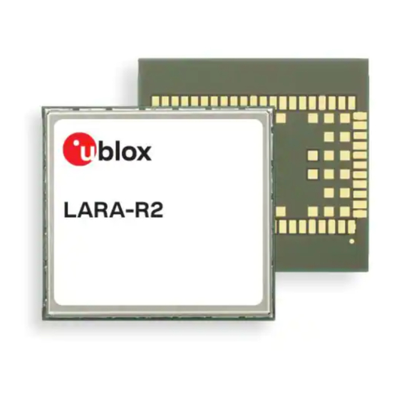
LARA-R2 series
LTE Cat 1 / EGPRS modules
System Integration Manual
Abstract
This document describes the features and the system integration of
LARA-R2 series multi-mode cellular modules.
These modules are a complete, cost efficient and performance
optimized LTE Cat 1 / 2G multi-mode solution covering up to three
LTE bands and up to two 2G GSM/EGPRS bands in the very small
and compact LARA form factor.
.
www.u-blox.com
UBX-16010573 - R02
Advertisement
Table of Contents

Related Manuals for u-blox LARA-R2 series


Summary of Contents for u-blox LARA-R2 series
- Page 1 System Integration Manual Abstract This document describes the features and the system integration of LARA-R2 series multi-mode cellular modules. These modules are a complete, cost efficient and performance optimized LTE Cat 1 / 2G multi-mode solution covering up to three LTE bands and up to two 2G GSM/EGPRS bands in the very small and compact LARA form factor.
- Page 2 The information contained herein is provided “as is” and u-blox assumes no liability for the use of the information. No warranty, either express or implied, is given, including but not limited, with respect to the accuracy, correctness, reliability and fitness for a particular purpose of the information.
-
Page 3: Preface
Application Notes: These documents provide guidelines and information on specific hardware and/or software topics on u-blox cellular modules. See Related documents for a list of application notes related to your cellular module. How to use this Manual The LARA-R2 series System Integration Manual provides the necessary information to successfully design in and configure these u-blox cellular modules. -
Page 4: Table Of Contents
LARA-R2 series - System Integration Manual Contents Preface ..........................3 Contents ..........................4 System description ....................... 7 Overview .............................. 7 Architecture ............................9 Pin-out ............................... 11 Operating modes ..........................16 Supply interfaces ..........................18 1.5.1 Module supply input (VCC) ......................18 1.5.2... - Page 5 Thermal guidelines ........................121 2.13 ESD guidelines ..........................122 2.13.1 ESD immunity test overview ...................... 122 2.14 Schematic for LARA-R2 series module integration ................. 123 2.15 Design-in checklist ........................124 2.15.1 Schematic checklist ........................124 2.15.2 Layout checklist ......................... 125 2.15.3...
- Page 6 LARA-R2 series - System Integration Manual Handling and soldering ................... 126 Packaging, shipping, storage and moisture preconditioning ............. 126 Handling ............................126 Soldering ............................127 3.3.1 Soldering paste.......................... 127 3.3.2 Reflow soldering ........................127 3.3.3 Optical inspection ........................128 3.3.4 Cleaning ............................
-
Page 7: System Description
1.1 Overview The LARA-R2 series comprises LTE Cat 1 / 2G multi-mode modules supporting up to three LTE bands and up to two 2G GSM/(E)GPRS bands for voice and/or data transmission in the very small LARA LGA form-factor (26.0 x 24.0 mm), easy to integrate in compact designs:... - Page 8 LARA-R2 modules provide Voice over LTE (VoLTE) as well as Circuit-Switched-Fall-Back (CSFB) audio capability LARA-R2 series modules support all the E-UTRA channel bandwidths for each operating band according to 3GPP TS 36.521-1 . GPRS/EDGE multi-slot class determines the number of timeslots available for upload and download and thus the speed at which data can be transmitted and received, with higher classes typically allowing faster data transfer rates.
-
Page 9: Architecture
External Reset V_INT (I/O) Figure 1: LARA-R2 series modules simplified block diagram LARA-R2 series modules internally consists of the RF, Baseband and Power Management sections here described with more details than the simplified block diagrams of Figure 1. RF section The RF section is composed of RF transceiver, PAs, LNAs, crystal oscillator, filters, duplexers and RF switches. - Page 10 LARA-R2 series - System Integration Manual Baseband and power management section The Baseband and Power Management section is composed of the following main elements: A mixed signal ASIC, which integrates Microprocessor for control functions DSP core for cellular Layer 1 and digital processing of Rx and Tx signal paths...
-
Page 11: Pin-Out
LARA-R2 series - System Integration Manual 1.3 Pin-out Table 3 lists the pin-out of the LARA-R2 series modules, with pins grouped by function. Function Pin Name Pin No Description Remarks Power 51, 52, 53 Module supply input VCC supply circuit affects the RF performance and compliance of the device integrating the module with applicable required certification schemes. - Page 12 LARA-R2 series - System Integration Manual Function Pin Name Pin No Description Remarks VSIM VSIM = 1.8 V / 3 V output as per the connected SIM type. SIM supply output See section 1.8 for functional description. See section 2.5 for external circuit design-in.
- Page 13 USB_D- USB Data Line D- USB interface for AT commands, data communication, FOAT, FW update by u-blox EasyFlash tool and diagnostic. 90 nominal differential impedance (Z 30 nominal common mode impedance (Z Pull-up or pull-down resistors and external series resistors as required by the USB 2.0 specifications [9] are part of the...
- Page 14 Remarks SDIO SDIO_D0 SDIO serial data [0] Not supported by “02” product versions. SDIO interface for communication with u-blox Wi-Fi module See section 1.9.5 for functional description. See section 2.6.5 for external circuit design-in. SDIO_D1 SDIO serial data [1] Not supported by “02” product versions.
- Page 15 See sections 1.13 and 2.9 RSVD 31, 97, 98 RESERVED pin Internally not connected. Leave unconnected. See sections 1.13 and 2.9 Table 3: LARA-R2 series modules pin definition, grouped by function UBX-16010573 - R02 Objective Specification System description Page 15 of 148...
-
Page 16: Operating Modes
LARA-R2 series - System Integration Manual 1.4 Operating modes LARA-R2 series modules have several operating modes. The operating modes defined in Table 4 and described in detail in Table 5 provide general guidelines for operation. General Status Operating Mode Definition... - Page 17 AT+UPSV command (see If power saving configuration is enabled by the AT+UPSV command, sections 1.5.1.3, 1.9.1.4 and to the u-blox AT the module automatically switches from active to idle-mode whenever Commands Manual [2]). possible and the module wakes up from idle to active-mode in the events listed above (see idle to active transition description).
-
Page 18: Supply Interfaces
V_BCKP Real Time Clock supply, V_INT digital interfaces supply and VSIM SIM card supply. During operation, the current drawn by the LARA-R2 series modules through the VCC pins can vary by several orders of magnitude. This ranges from the pulse of current consumption during GSM transmitting bursts at maximum power level in connected-mode (as described in section 1.5.1.2) to the low current consumption... - Page 19 VCC supply circuit compliant to the requirements listed in Table 6. VCC supply circuit affects the RF compliance of the device integrating LARA-R2 series modules with applicable required certification schemes as well as antenna circuit design. Compliance is guaranteed if the VCC requirements summarized in the Table 6 are fulfilled.
- Page 20 RF power control level (approximately 2 W or 33 dBm in the Tx slot/burst), the current consumption can reach an high peak / pulse (see LARA-R2 series Data Sheet [1]) for 576.9 µs (width of the transmit slot/burst) with a periodicity of 4.615 ms (width of 1 frame = 8 slots/burst), so with a 1/8 duty cycle according to GSM TDMA (Time Division Multiple Access).
- Page 21 The multi-slot transmission power can be further reduced by configuring the actual Multi-Slot Power Reduction profile with the dedicated AT command, AT+UDCONF=40 (see the u-blox AT Commands Manual [2]). If the module transmits in GPRS class 12 in the 850 or 900 MHz bands, at the maximum RF power control level, the current consumption can reach a quite high peak but lower than the one achievable in 2G single-slot mode.
- Page 22 (approximately 250 mW or 24 dBm), the average current drawn by the module at the VCC pins is considerable (see the “Current consumption” section in LARA-R2 series Data Sheet [1]). At the lowest output RF power (approximately 0.1 µW or –40 dBm), the current drawn by the internal power amplifier is strongly reduced and the total current drawn by the module at the VCC pins is due to baseband processing and transceiver activity.
- Page 23 The power saving configuration is by default disabled, but it can be enabled using the appropriate AT command (see u-blox AT Commands Manual [2], AT+UPSV command). When power saving is enabled, the module automatically enters low power idle-mode whenever possible, reducing current consumption.
- Page 24 Power saving configuration is by default disabled, or it can be disabled using the appropriate AT command (see u-blox AT Commands Manual [2], AT+UPSV command). When power saving is disabled, the module does not automatically enter idle-mode whenever possible: the module remains in active-mode.
-
Page 25: Rtc Supply Input/Output (V_Bckp)
1.5.2 RTC supply input/output (V_BCKP) The V_BCKP pin of LARA-R2 series modules connects the supply for the Real Time Clock (RTC) and Power-On internal logic. This supply domain is internally generated by a linear LDO regulator integrated in the Power Management Unit, as described in Figure 10. -
Page 26: Generic Digital Interfaces Supply Output (V_Int)
1.5.3 Generic digital interfaces supply output (V_INT) The V_INT output pin of the LARA-R2 series modules is connected to an internal 1.8 V supply with current capability specified in the LARA-R2 series Data Sheet [1]. This supply is internally generated by a switching step- down regulator integrated in the Power Management Unit and it is internally used to source the generic digital I/O interfaces of the cellular module, as described in Figure 11. -
Page 27: System Function Interfaces
LARA-R2 series - System Integration Manual 1.6 System function interfaces 1.6.1 Module power-on When the LARA-R2 series modules are in the not-powered mode (switched off, i.e. the VCC module supply is not applied), they can be switched on as following: ... - Page 28 The internal reset signal is held low: the baseband core and all the digital pins are held in the reset state. The reset state of all the digital pins is reported in the pin description table of LARA-R2 series Data Sheet [1].
-
Page 29: Module Power-Off
(V_INT) is switched off by the module. An abrupt hardware shutdown occurs on LARA-R2 series modules when a low level is applied on RESET_N pin. In this case, the current parameter settings are not saved in the module’s non-volatile memory and a proper network detach is not performed. - Page 30 The Internal Reset signal is not available on a module pin, but the application can monitor the V_INT pin to sense the end of the LARA-R2 series power-off sequence. The duration of each phase in the LARA-R2 series modules’ switch-off routines can largely vary depending on the application / network settings and the concurrent module activities.
-
Page 31: Module Reset
An abrupt hardware reset occurs on LARA-R2 series modules when a low level is applied on the RESET_N input pin for a specific time period. In this case, the current parameter settings are not saved in the module’s non- volatile memory and a proper network detach is not performed. -
Page 32: Antenna Interface
The ANT2 represents the secondary RF input for the reception of the LTE RF signals for the Down-Link Rx diversity radio technology supported by LARA-R2 series modules as required feature for LTE category 1 UEs. The ANT2 pin has a nominal characteristic impedance of 50 and must be connected to the secondary Rx antenna through a 50 ... - Page 33 The impedance of the antenna RF connection must match the 50 impedance of the ANT2 port. Frequency Range See the LARA-R2 series Data Sheet [1] The required frequency range of the antennas connected to ANT2 port depends on the operating bands of the used cellular module and the used Mobile Network.
-
Page 34: Antenna Detection Interface (Ant_Det)
Commands Manual [2] for more details on this feature. The ANT_DET pin generates a DC current (for detailed characteristics see the LARA-R2 series Data Sheet [1]) and measures the resulting DC voltage, thus determining the resistance from the antenna connector provided on the application board to GND. -
Page 35: Data Communication Interfaces
LARA-R2 series modules’ UART interface is by default configured in AT command mode: the module waits for AT command instructions and interprets all the characters received as commands to execute. See the u-blox AT Commands Manual [2] for the definition of the command mode, data mode, and online command mode. UBX-16010573 - R02... - Page 36 LARA-R2 series - System Integration Manual All the functionalities supported by LARA-R2 series modules can be set and configured by AT commands: AT commands according to 3GPP TS 27.007 [6], 3GPP TS 27.005 [7], 3GPP TS 27.010 [8] ...
- Page 37 OFF state if the line is not activated by the DTE: an active pull-up is enabled inside the module on the TXD input. See the u-blox AT Commands Manual [2] for the definition of the command mode, data mode, and online command mode Not supported by “02” product versions Refer to the pin description table in the LARA-R2 series Data Sheet [1].
- Page 38 If AT&S0 is set, the DSR module output line is set by default to the ON state (low level) at UART initialization and is then always held in the ON state. See the u-blox AT Commands Manual [2] for the definition of the command mode, data mode, and online command mode UBX-16010573 - R02...
- Page 39 If AT&C0 is set, the DCD module output line is set by default to the ON state (low level) at UART initialization and is then always held in the ON state. See the u-blox AT Commands Manual [2] for the definition of the command mode, data mode, and online command mode UBX-16010573 - R02...
- Page 40 The RI line can notify an SMS arrival. When the SMS arrives, the RI line switches from OFF to ON for 1 s (see Figure 18), if the feature is enabled by the AT+CNMI command (see the u-blox AT Commands Manual [2]).
- Page 41 The power saving configuration is controlled by the AT+UPSV command (for the complete description, see u-blox AT Commands Manual [2]). When power saving is enabled, the module automatically enters low power idle-mode whenever possible, and otherwise the active-mode is maintained by the module (see section 1.4 for definition and description of module operating modes referred to in this section).
- Page 42 LARA-R2 series - System Integration Manual AT+UPSV HW flow control RTS line DTR line Communication during idle-mode and wake up Enabled (AT&K3) Data sent by the DTE is correctly received by the module. Data sent by the module is correctly received by the DTE.
- Page 43 DTE over the UART. When the AT+UPSV=3 configuration is enabled, the DTR input line can still be used by the DTE to control the module behavior according to AT&D command configuration (see u-blox AT commands Manual [2]). UBX-16010573 - R02...
- Page 44 LARA-R2 series - System Integration Manual Wake up via data reception The UART wake up via data reception consists of a special configuration of the module TXD input line that causes the system wake-up when a low-to-high transition occurs on the TXD input line. In particular, the UART is enabled and the module switches from the low power idle-mode to active-mode within ~20 ms from the first character received: this is the system “wake up time”.
- Page 45 Channel 6: GNSS data tunneling The GNSS data tunneling channel is not supported by “02” product versions. See the u-blox AT Commands Manual [2] for the definition of the command mode, data mode, and online command mode. UBX-16010573 - R02...
-
Page 46: Usb Interface
USB profile identified by this VID and PID combination. See the u-blox AT Commands Manual [2] for the definition of the command mode, data mode, and online command mode. UBX-16010573 - R02... - Page 47 Interface 10 Abstract Control Model EndPoint Transfer: Interrupt Interface 11 Data EndPoint Transfer: Bulk EndPoint Transfer: Bulk Figure 22: LARA-R2 series USB End-Points summary for the default USB profile configuration UBX-16010573 - R02 Objective Specification System description Page 47 of 148...
- Page 48 Windows Embedded Compact 7 Windows Embedded Compact 2013 The module firmware can be upgraded over the USB interface by means of the FOAT feature, or using the u-blox EasyFlash tool (for more details see Firmware Update Application Note [23]. 1.9.2.3...
-
Page 49: Hsic Interface
u-blox AT commands (for the complete list and syntax see the u-blox AT Commands Manual [2]) See the u-blox AT Commands Manual [2] for the definition of the command mode, data mode, and online command mode. UBX-16010573 - R02... -
Page 50: Ddc (I C) Interface
I C bus specifications [11]. u-blox has implemented special features to ease the design effort required for the integration of a u-blox cellular module with a u blox GNSS receiver. Combining a u-blox cellular module with a u-blox GNSS receiver allows designers to have full access to the... -
Page 51: Sdio Interface
VCC supply of the GNSS receiver is disabled. This enables the u-blox positioning receiver to recover from a power breakdown with either a hot start or a warm start (depending on the duration of the GNSS receiver VCC outage) and to maintain the configuration settings saved in the backup RAM. -
Page 52: Audio Interface
I2S_CLK clock input/output, I2S_WA world alignment / synchronization signal input/output), which can be configured by AT command for digital audio communication with external digital audio devices as an audio codec (for more details see the u-blox AT Commands Manual [2], +UI2S AT command). The I S interface can be alternatively set in different modes, by <I2S_mode>... -
Page 53: Clock Output
GPIO1-GPIO3 Table 12: LARA-R2 series GPIO custom functions configuration 1.13 Reserved pins (RSVD) LARA-R2 series modules have pins reserved for future use, named RSVD: they can all be left unconnected on the application board, except the RSVD pin number 33 that must be externally connected to ground Not supported by “02”... -
Page 54: System Features
(i.e. configuring the module in “airplane mode” by means of the +CFUN AT command) in order to reduce power consumption and monitoring the environment at constant periods (for more details see the u-blox AT Commands Manual [2], +UCD AT command). UBX-16010573 - R02... -
Page 55: Dual Stack Ipv4/Ipv6
For more details about embedded TCP/IP and UDP/IP functionalities see the u-blox AT Commands Manual [2] 1.14.6 FTP LARA-R2 series provide embedded File Transfer Protocol (FTP) services. Files are read and stored in the local file system of the module. -
Page 56: Ssl/Tls
LARA-R2 series - System Integration Manual 1.14.8 SSL/TLS LARA-R2 series modules support the Secure Sockets Layer (SSL) / Transport Layer Security (TLS) with certificate key sizes up to 4096 bits to provide security over the FTP and HTTP protocols. The SSL/TLS support provides different connection security aspects: ... -
Page 57: Bearer Independent Protocol
AT command (see the u-blox AT Commands Manual [2]). LARA-R2 series cellular modules act as a stand-alone AssistNow client, making AssistNow available with no additional requirements for resources or software integration on an external host micro controller. Full access to... -
Page 58: Hybrid Positioning And Celllocate
® visible to the specific device. To estimate its position the u-blox cellular module sends the CellLocate server the parameters of network cells visible to it using a UDP connection. In return the server provides the estimated ®... - Page 59 Hybrid positioning With u-blox hybrid positioning technology, u-blox cellular modules can be triggered to provide their current ® position using either a u-blox GNSS receiver or the position estimated from CellLocate .
-
Page 60: Wi-Fi Integration
Full access to u-blox short range communication Wi-Fi modules is available through a dedicated SDIO interface (see sections 1.9.5 and 2.6.5). This means that combining a LARA-R2 series cellular module with a u-blox short range communication module gives designers full access to the Wi-Fi module directly via the cellular module, so that a second interface connected to the Wi-Fi module is not necessary. -
Page 61: Smart Temperature Management
Smart Temperature Supervisor (STS) The Smart Temperature Supervisor is activated and configured by a dedicated AT+USTS command. See u-blox AT Commands Manual [2] for more details. An URC indication is provided once the feature is enabled and at the module power on. - Page 62 LARA-R2 series - System Integration Manual Figure 24 shows the flow diagram implemented for the Smart Temperature Supervisor. IF STS enabled Feature enabled Feature disabled: (full logic or no action indication only) Read temperature <Ti<t Temperature is within normal operating range...
-
Page 63: Power Saving
The connected USB host forces a remote wakeup of the module as USB device (see 1.9.2.4) The connected u-blox GNSS receiver forces a wakeup of the cellular module using the GNSS Tx data ready function over GPIO3 (see 1.9.4) ... -
Page 64: Design-In
2 Design-in 2.1 Overview For an optimal integration of LARA-R2 series modules in the final application board follow the design guidelines stated in this section. Every application circuit must be properly designed to guarantee the correct functionality of the related interface, however a number of points require higher attention during the design of the application device. -
Page 65: Supply Interfaces
(low impedance) connection to external ground can minimize power loss and improve RF and thermal performance. LARA-R2 series modules must be supplied through the VCC pins by a proper DC power supply that should comply with the module VCC requirements summarized in Table 6. - Page 66 The usage of a regulator or a battery not able to support the highest peak of VCC current consumption specified in the LARA-R2 series Data Sheet [1] is generally not recommended. However, if the selected regulator or battery is not able to support the highest peak current of the module, it must be able to support with adequate margin at least the highest averaged current consumption value specified in the LARA-R2 series Data Sheet [1].
- Page 67 LARA-R2 series - System Integration Manual Figure 26 and the components listed in Table 19 show an example of a high reliability power supply circuit, where the module VCC is supplied by a step-down switching regulator capable of delivering to VCC pins the specified maximum peak / pulse current, with low output ripple and with fixed switching frequency in PWM mode operation greater than 1 MHz.
- Page 68 LARA-R2 series - System Integration Manual Figure 27 and the components listed in Table 20 show an example of a low cost power supply circuit, where the VCC module supply is provided by a step-down switching regulator capable of delivering to VCC pins the specified maximum peak / pulse current, transforming a 12 V supply input.
- Page 69 LARA-R2 series - System Integration Manual 2.2.1.3 Guidelines for VCC supply circuit design using a Low Drop-Out (LDO) linear regulator The use of a linear regulator is suggested when the difference from the available supply rail and the VCC value is low: linear regulators provide high efficiency when transforming a 5 V supply to a voltage value within the module VCC normal operating range.
- Page 70 LARA-R2 series - System Integration Manual Figure 29 and the components listed in Table 22 show an example of a low cost power supply circuit, where the VCC module supply is provided by an LDO linear regulator capable of delivering the specified highest peak / pulse current, with proper power handling capability.
- Page 71 VCC pins must be capable of delivering a pulse current as the maximum peak current consumption during Tx burst at maximum Tx power specified in LARA-R2 series Data Sheet [1] and must be capable of extensively delivering a DC current as the maximum average current consumption specified in LARA-R2 series Data Sheet [1].
- Page 72 GSM call (when current consumption on the VCC supply can rise up as specified in the LARA-R2 series Data Sheet [1]), place a bypass capacitor with large capacitance (at least 100 µF) and low ESR near the VCC pins, for example:...
- Page 73 2.2.1.8 Guidelines for external battery charging circuit LARA-R2 series modules do not have an on-board charging circuit. Figure 32 provides an example of a battery charger design, suitable for applications that are battery powered with a Li-Ion (or Li-Polymer) cell.
- Page 74 LARA-R2 series - System Integration Manual the module. Battery charging is completely managed by the STMicroelectronics L6924U Battery Charger IC that, from a USB power source (5.0 V typ.), charges as a linear charger the battery, in three phases: ...
- Page 75 LARA-R2 series - System Integration Manual suitable charger / regulator with integrated power path management function to supply the module and the whole device while simultaneously and independently charging the battery. Figure 33 reports a simplified block diagram circuit showing the working principle of a charger / regulator with integrated power path management function.
- Page 76 LARA-R2 series - System Integration Manual Fast-charge constant current: the battery is charged with the maximum current, configured by the value of an external resistor to a value suitable for the application Constant voltage: when the battery voltage reaches the regulated output voltage (4.2 V), the current is progressively reduced until the charge termination is done.
- Page 77 2.2.1.10 Guidelines for removing VCC supply As described in section 1.6.2 and Figure 14, the VCC supply can be removed after the end of LARA-R2 series modules internal power-off sequence, which has to be properly started sending the AT+CPWROFF command (see u-blox AT Commands Manual [2]).
- Page 78 RF signal. This is more likely to happen with switching DC-DC converters, in which case it is better to select the highest operating frequency for the switcher and add a large L-C filter before connecting to the LARA-R2 series modules in the worst case. ...
-
Page 79: Rtc Supply (V_Bckp)
V_BCKP (specified in the Input characteristics of Supply/Power pins table in the LARA-R2 series Data Sheet [1]). The connection of the battery to V_BCKP should be done with a suitable series resistor for a rechargeable battery, or with an appropriate series diode for a non-rechargeable battery. - Page 80 RAM when the VCC supply of the cellular module is within its operating range and the VCC supply of the GNSS receiver is disabled. This enables the u-blox GNSS receiver to recover from a power breakdown with either a hot start or a warm start (depending on the duration of the positioning VCC outage) and to maintain the configuration settings saved in the backup RAM.
-
Page 81: Interface Supply (V_Int)
2.2.3 Interface supply (V_INT) 2.2.3.1 Guidelines for V_INT circuit design LARA-R2 series provide the V_INT generic digital interfaces 1.8 V supply output, which can be mainly used to: Indicate when the module is switched on (see sections 1.6.1, 1.6.2 for more details) ... -
Page 82: System Functions Interfaces
The power-on circuit (PWR_ON) requires careful layout since it is the sensitive input available to switch on the LARA-R2 series modules. It is required to ensure that the voltage level is well defined during operation and no transient noise is coupled on this line, otherwise the module might detect a spurious power-on request. -
Page 83: Module Reset (Reset_N)
2.3.2.1 Guidelines for RESET_N circuit design LARA-R2 series RESET_N is equipped with an internal pull-up to the V_BCKP supply as described in Figure 38. An external pull-up resistor is not required. If connecting the RESET_N input to a push button, the pin will be externally accessible on the application device. -
Page 84: Module / Host Configuration Selection
Selection of module / host configuration over HOST_SELECT is not supported by “02” product versions. LARA-R2 series modules include one pin (HOST_SELECT) to select the module / host application processor configuration: the pin is available to select, enable, connect, disconnect and subsequently re-connect the HSIC (USB High-Speed Inter-Chip) interface. -
Page 85: Antenna Interface
RF compliance of the device integrating LARA-R2 series modules with all the applicable required certification schemes depends on antennas radiating performance. - Page 86 LARA-R2 series - System Integration Manual Radiation performance depends on the whole PCB and antenna system design, including product mechanical design and usage. Antennas should be selected with optimal radiating performance in the operating bands according to the mechanical specifications of the PCB and the whole product.
- Page 87 LARA-R2 series - System Integration Manual Guidelines for RF transmission line design Any RF transmission line, such as the ones from the ANT1 and ANT2 pads up to the related antenna connector or up to the related internal antenna pad, must be designed so that the characteristic impedance is as close as possible to 50 .
- Page 88 LARA-R2 series - System Integration Manual the dielectric constant of the dielectric material (e.g. dielectric constant of the FR-4 dielectric material in Figure 40 and Figure 41) the gap from the transmission line to the adjacent ground plane on the same layer of the transmission line (e.g.
- Page 89 LARA-R2 series - System Integration Manual Guidelines for RF termination design RF terminations must provide a characteristic impedance of 50 as well as the RF transmission lines up to the RF terminations themselves, to match the characteristic impedance of the ANT1 / ANT2 ports of the modules.
- Page 90 LARA-R2 series - System Integration Manual Examples of antennas Table 31 lists some examples of possible internal on-board surface-mount antennas. Manufacturer Part Number Product Name Description Taoglas PA.710.A Warrior GSM / WCDMA / LTE SMD Antenna 698..960 MHz, 1710..2170 MHz, 2300..2400 MHz, 2490..2690 MHz 40.0 x 6.0 x 5.0 mm...
- Page 91 LARA-R2 series - System Integration Manual Table 33 lists some examples of possible external antennas. Manufacturer Part Number Product Name Description Taoglas GSA.8827.A.101111 Phoenix GSM / WCDMA / LTE adhesive-mount antenna with cable and SMA(M) 698..960 MHz, 1575.42 MHz, 1710..2170 MHz, 2490..2690 MHz 105 x 30 x 7.7 mm...
-
Page 92: Antenna Detection Interface (Ant_Det)
LARA-R2 series - System Integration Manual 2.4.2 Antenna detection interface (ANT_DET) 2.4.2.1 Guidelines for ANT_DET circuit design Figure 43 and Table 34 describe the recommended schematic / components for the antennas detection circuit that must be provided on the application board and for the diagnostic circuit that must be provided on the antennas’... - Page 93 15 k diagnostic resistor is used) indicate that the antenna is properly connected. Values close to the measurement range maximum limit (approximately 50 k) or an open-circuit “over range” report (see u-blox AT Commands Manual [2]) means that that the antenna is not connected or the RF cable is broken. ...
-
Page 94: Sim Interface
LARA-R2 series - System Integration Manual 2.5 SIM interface 2.5.1.1 Guidelines for SIM circuit design Guidelines for SIM cards, SIM connectors and SIM chips selection The ISO/IEC 7816, the ETSI TS 102 221 and the ETSI TS 102 671 specifications define the physical, electrical and... - Page 95 LARA-R2 series - System Integration Manual Guidelines for single SIM card connection without detection A removable SIM card placed in a SIM card holder has to be connected to the SIM card interface of LARA-R2 series modules as described in Figure 44, where the optional SIM detection feature is not implemented.
- Page 96 LARA-R2 series - System Integration Manual Guidelines for single SIM chip connection A solderable SIM chip (M2M UICC Form Factor) has to be connected the SIM card interface of LARA-R2 series modules as described in Figure 45. Follow these guidelines connecting the module to a solderable SIM chip without SIM presence detection: ...
- Page 97 LARA-R2 series - System Integration Manual Guidelines for single SIM card connection with detection A removable SIM card placed in a SIM card holder must be connected to the SIM card interface of LARA-R2 series modules as described in Figure 46, where the optional SIM card detection feature is implemented.
- Page 98 Guidelines for dual SIM card / chip connection Two SIM card / chip can be connected to the SIM interface of LARA-R2 series modules as described in Figure 47. LARA-R2 series modules do not support the usage of two SIM at the same time, but two SIM can be populated on the application board, providing a proper switch to connect only the first or only the second SIM at a time to the SIM interface of the modules, as described in Figure 47.
- Page 99 The layout of the SIM card interface lines (VSIM, SIM_CLK, SIM_IO, SIM_RST) may be critical if the SIM card is placed far away from the LARA-R2 series modules or in close proximity to the RF antenna: these two cases should be avoided or at least mitigated as described below.
-
Page 100: Data Communication Interfaces
LARA-R2 series - System Integration Manual 2.6 Data communication interfaces 2.6.1 UART interface 2.6.1.1 Guidelines for UART circuit design Providing the full RS-232 functionality (using the complete V.24 link) If RS-232 compatible signal levels are needed, two different external voltage translators can be used to provide full RS-232 (9 lines) functionality: e.g. - Page 101 LARA-R2 series - System Integration Manual Providing the TXD, RXD, RTS, CTS and DTR lines only (not using the complete V.24 link) If the functionality of the DSR, DCD and RI lines is not required, or the lines are not available: ...
- Page 102 Connect the module DTR input to GND using a 0 series resistor, since it may be useful to set DTR active if not specifically handled (see u-blox AT Commands Manual [2], &D, S0, +CSGT, +CNMI AT commands) ...
- Page 103 Connect the module DTR input to GND using a 0 series resistor, since it may be useful to set DTR active if not specifically handled (see u-blox AT Commands Manual [2], &D, S0, +CSGT, +CNMI AT commands) ...
- Page 104 LARA-R2 series - System Integration Manual Additional considerations If a 3.0 V Application Processor (DTE) is used, the voltage scaling from any 3.0 V output of the DTE to the apposite 1.8 V input of the module (DCE) can be implemented, as an alternative low-cost solution, by means of an appropriate voltage divider.
-
Page 105: Usb Interface
The USB interface of the module is enabled only if a valid voltage is detected by the VUSB_DET input (see the LARA-R2 series Data Sheet [1]). Neither the USB interface, nor the whole module is supplied by the VUSB_DET input: the VUSB_DET senses the USB supply voltage and absorbs few microamperes. - Page 106 LARA-R2 series - System Integration Manual 2.6.2.2 Guidelines for USB layout design The USB_D+ / USB_D- lines require accurate layout design to achieve reliable signaling at the high speed data rate (up to 480 Mb/s) supported by the USB serial interface.
-
Page 107: Hsic Interface
(HSIC_STRB), intended to be directly connected to the Data and Strobe pins of the compatible USB High-Speed Inter-Chip host mounted on the same PCB of the LARA-R2 series module, without using connectors / cables, as described in Figure 59. - Page 108 LARA-R2 series - System Integration Manual 2.6.3.2 Guidelines for HSIC layout design HSIC lines require accurate layout design to achieve reliable signaling at high speed data rate (up to 480 Mb/s), as supported by the HSIC serial interface: signal integrity may be degraded if PCB layout is not optimal, especially when the HSIC lines are very long.
-
Page 109: Ddc (I C) Interface
C-bus slaves as an audio codec. Beside the general considerations reported below, see: the following parts of this section for specific guidelines for the connection to u-blox GNSS receivers. the section 2.7.1 for an application circuit example with an external audio codec I C-bus slave. - Page 110 Figure 60 shows an application circuit for connecting the cellular module to a u-blox 1.8 V GNSS receiver: The SDA and SCL pins of the cellular module are directly connected to the related pins of the u-blox 1.8 V GNSS receiver, with appropriate pull-up resistors connected to the 1.8 V GNSS supply enabled after the V_INT supply of the I C pins of the cellular module.
- Page 111 Figure 61 illustrates an alternative solution as supply for u-blox 1.8 V GNSS receivers: the V_INT 1.8 V regulated supply output of the cellular module can be used to supply a u-blox 1.8 V GNSS receiver of the u-blox 6 generation (or any newer u-blox GNSS receiver generation) instead of using an external voltage regulator as shown in the previous Figure 60.
- Page 112 3.0 V supply can be ramped up before the V_INT 1.8 V cellular supply), with proper pull-up resistors. The GPIO2 is connected to the active-high enable pin of the voltage regulator that supplies the u-blox 3.0 V GNSS receiver providing the “GNSS supply enable” function. A pull-down resistor is provided to avoid a switch on of the positioning receiver when the cellular module is switched off or in the reset state.
-
Page 113: Sdio Interface
SDIO_D3, SDIO_CLK, SDIO_CMD) designed to communicate with an external u-blox short range Wi-Fi module. Combining a u-blox cellular module with a u-blox short range communication module gives designers full access to the Wi-Fi module directly via the cellular module, so that a second interface connected to the Wi-Fi module is not necessary. -
Page 114: Audio Interface
The opposite role: slave or master role, as LARA-R2 series modules may act as master or slave The same mode and frame format: PCM / short synch mode or Normal I S / long synch mode with data in 2’s complement notation... - Page 115 S master) is connected to the related pins of the external audio codec (I S slave). The GPIO6 of the LARA-R2 series module (that provides a suitable digital output clock) is connected to the clock input of the external audio codec to provide clock reference. ...
- Page 116 LARA-R2 series - System Integration Manual Reference Description Part Number – Manufacturer 100 nF Capacitor Ceramic X5R 0402 10% 10V GRM155R71C104KA01 – Murata C2, C4, C5, C6 1 µF Capacitor Ceramic X5R 0402 10% 6.3 V GRM155R60J105KE19 – Murata 10 µF Capacitor Ceramic X5R 0603 20% 6.3 V GRM188R60J106ME47 –...
- Page 117 LARA-R2 series - System Integration Manual Keep ground separation from microphone lines to other noisy signals. Use an intermediate ground layer or vias wall for coplanar signals. In case of external audio device providing differential microphone input, route microphone signal lines as a differential pair embedded in ground to reduce differential noise pick-up.
-
Page 118: General Purpose Input/Output (Gpio)
LARA-R2 series - System Integration Manual 2.8 General Purpose Input/Output (GPIO) 2.8.1.1 Guidelines for GPIO circuit design A typical usage of LARA-R2 series modules’ GPIOs can be the following: Network indication provided over GPIO1 pin (see Figure 64 / Table 48 below) ... -
Page 119: Reserved Pins (Rsvd)
LARA-R2 series - System Integration Manual 2.9 Reserved pins (RSVD) LARA-R2 series modules have pins reserved for future use, marked as RSVD. All the RSVD pins are to be left unconnected on the application board except the following RSVD pin, as described in Figure 65: ... -
Page 120: Module Footprint And Paste Mask
F1’’ F2’ F2’’ H’ H’ H’’ H’’ J’ J’ J’’ J’’ Figure 66: LARA-R2 series modules suggested footprint and paste mask (application board top view) Parameter Value Parameter Value Parameter Value 26.0 mm F2’’ 5.00 mm 2.75 mm 24.0 mm 1.10 mm... -
Page 121: Thermal Guidelines
GND pads of the LARA-R2 series LGA modules and dissipated over the backside of the application board. -
Page 122: Esd Guidelines
Data Sheet [1]. Special precautions are required when handling: see section 3.2 for handling guidelines. 2.13.1 ESD immunity test overview The immunity of devices integrating LARA-R2 series modules to Electro-Static Discharge (ESD) is part of the Electro-Magnetic Compatibility (EMC) conformity, which is required for products bearing the CE marking, compliant with the R&TTE Directive (99/5/EC), the EMC Directive (89/336/EEC) and the Low Voltage Directive... -
Page 123: Schematic For Lara-R2 Series Module Integration
2.14 Schematic for LARA-R2 series module integration Figure 67 is an example of a schematic diagram where a LARA-R2 series cellular module “02” product version is integrated into an application board, using all the available interfaces and functions of the module. -
Page 124: Design-In Checklist
Provide proper precautions for ESD immunity as required on the application board. Do not apply voltage to any generic digital interface pin of LARA-R2 series modules before the switch-on of the generic digital interface supply source (V_INT). ... -
Page 125: Layout Checklist
SIM signals, high-speed digital lines such as SDIO, USB and other data lines). Optimize placement for minimum length of RF line. Check the footprint and paste mask designed for LARA-R2 series module as illustrated in section 2.11. VCC line should be wide and as short as possible. ... -
Page 126: Handling And Soldering
3.1 Packaging, shipping, storage and moisture preconditioning For information pertaining to LARA-R2 series reels / tapes, Moisture Sensitivity levels (MSD), shipment and storage information, as well as drying for preconditioning, see the LARA-R2 series Data Sheet [1] and the u-blox Package Information Guide [25]. -
Page 127: Soldering
LARA-R2 series - System Integration Manual 3.3 Soldering 3.3.1 Soldering paste Use of "No Clean" soldering paste is strongly recommended, as it does not require cleaning after the soldering process has taken place. The paste listed in the example below meets these criteria. -
Page 128: Optical Inspection
Figure 68: Recommended soldering profile LARA-R2 series modules must not be soldered with a damp heat process. 3.3.3 Optical inspection After soldering the LARA-R2 series modules, inspect the modules optically to verify that the module is properly aligned and centered. 3.3.4 Cleaning Cleaning the soldered modules is not recommended. -
Page 129: Repeated Reflow Soldering
Certain applications employ a conformal coating of the PCB using HumiSeal or other related coating products. These materials affect the RF properties of the LARA-R2 series modules and it is important to prevent them from flowing into the module. The RF shields do not provide 100% protection for the module from coating liquids with low viscosity, therefore care is required in applying the coating. -
Page 130: Approvals
The required certification scheme approvals and relative testing specifications differ depending on the country or the region where the device that integrates LARA-R2 series modules must be deployed, on the relative vertical market of the device, on type, features and functionalities of the whole application device, and on the network operators where the device must operate. -
Page 131: Us Federal Communications Commission Notice
Manufacturers of mobile or fixed devices incorporating the LARA-R2 series modules are authorized to use the FCC Grants of the LARA-R2 series modules for their own final products according to the conditions referenced in the certificates. -
Page 132: Industry Canada Notice
The gain of the system antenna(s) used for the LARA-R2 series modules (i.e. the combined transmission line, connector, cable losses and radiating element gain) must not exceed 7.6 dBi (1700 MHz , i.e. - Page 133 Informations concernant l'exposition aux fréquences radio (RF) La puissance de sortie émise par l’appareil de sans fil u-blox Cellular Module est inférieure à la limite d'exposition aux fréquences radio d'Industrie Canada (IC). Utilisez l’appareil de sans fil u-blox Cellular Module de façon à...
-
Page 134: R&Tted / Red And European Conformance Ce Mark
Pour des informations supplémentaires concernant l'exposition aux RF au Canada rendez-vous sur: http://www.ic.gc.ca/eic/site/smt-gst.nsf/fra/sf08792.html IMPORTANT: les fabricants d'applications portables contenant les modules LARA-R2 series doivent faire certifier leur produit final et déposer directement leur candidature pour une certification FCC ainsi que pour un certificat Industrie Canada délivré par l'organisme chargé de ce type d'appareil portable. -
Page 135: Product Testing
5 Product testing 5.1 u-blox in-series production test u-blox focuses on high quality for its products. All units produced are fully tested automatically in production line. Stringent quality control process has been implemented in the production line. Defective units are analyzed in detail to improve the production quality. -
Page 136: Test Parameters For Oem Manufacturer
This test should be performed after data connection has been established. AT+CSQ is the typical AT command used to check signal quality in term of RSSI. See the u-blox AT Commands Manual [2] for detail usage of the AT command. - Page 137 The use of this feature is intended for testing purpose in controlled environments by qualified user and must not be used during the normal module operation. Follow instructions suggested in u-blox documentation. u-blox assumes no responsibilities for the inappropriate use of this feature.
-
Page 138: Appendix
A Migration between SARA-U2 and LARA-R2 A.1 Overview Migrating between u-blox SARA-U2 series 3G / 2G cellular modules and LARA-R2 series LTE Cat 1 / 2G cellular modules is a straightforward procedure that allows customers to take maximum advantage of their hardware and software investments. - Page 139 SARA, LARA, LISA and TOBY modules have been developed to ensure layout compatibility. With the u-blox “nested design” solution, any SARA, LARA, LISA or TOBY module can be alternatively mounted on the same space of a single “nested” application board as described in Figure 72, enabling straightforward development of products supporting different cellular radio access technologies.
- Page 140 ● = supported by all product versions ■ = supported by all product versions except version ‘02’ Table 51: Summary of SARA-U2 and LARA-R2 series modules interfaces Figure 74 summarizes the LTE, 3G and 2G operating frequency bands of SARA-U2 and LARA-R2 series modules. VIII VIII...
-
Page 141: Pin-Out Comparison Between Sara-U2 And Lara-R2
LARA-R2 series - System Integration Manual A.2 Pin-out comparison between SARA-U2 and LARA-R2 SARA-U2 LARA-R2 Pin No Pin Name Description Pin Name Description Remarks for migration Ground Ground V_BCKP RTC Supply I/O V_BCKP RTC Supply I/O No functional difference Output characteristics: Output characteristics: 1.8 V typ, 3 mA max... - Page 142 For further details regarding the characteristics, capabilities, usage or settings applicable for each interface of the SARA-U2 and LARA-R2 series modules, see LARA-R2 series Data Sheet [1], SARA-U2 series Data Sheet [27], SARA-G3 / SARA-U2 series System Integration Manual [28], u-blox AT Commands Manual [2] and Nested Design Application Note [26].
-
Page 143: Schematic For Sara-U2 And Lara-R2 Integration
A.3 Schematic for SARA-U2 and LARA-R2 integration Figure 75 shows an example of schematic diagram where a SARA-U2 or a LARA-R2 series module can be integrated into the same application board, using all the available interfaces and functions of the modules. The different mounting options for the external parts are herein remarked according to the functions supported by each module. -
Page 144: B Glossary
LARA-R2 series - System Integration Manual B Glossary 3GPP 3rd Generation Partnership Project 8-PSK 8 Phase-Shift Keying modulation 16QAM 16-state Quadrature Amplitude Modulation Abstract Control Model Analog to Digital Converter Application Processor ASIC Application-Specific Integrated Circuit AT Command Interpreter Software Subsystem, or attention... - Page 145 Low Power Double Data Rate synchronous dynamic RAM memory Long Term Evolution Modulation Coding Scheme Not Applicable Network Control Model Original Equipment Manufacturer device: an application device integrating a u-blox cellular module Over The Air Power Amplifier Pulse Code Modulation Pulse Frequency Modulation...
-
Page 146: Related Documents
AT Commands Manual, Docu No UBX-13002752 u-blox EVK-R2xx User Guide, Docu No UBX-16016088 u-blox Windows Embedded OS USB Driver Installation Application Note, Docu No UBX-14003263 ITU-T Recommendation V.24 - 02-2000 - List of definitions for interchange circuits between the Data Terminal Equipment (DTE) and the Data Circuit-terminating Equipment (DCE). -
Page 147: Revision History
LARA-R2 series - System Integration Manual Revision history Revision Date Name Status / Comments 20-Sep-2016 sses Initial release UBX-16010573 - R02 Objective Specification Revision history Page 147 of 148... -
Page 148: Contact
LARA-R2 series - System Integration Manual Contact For complete contact information visit us at www.u-blox.com. u-blox Offices North, Central and South America Headquarters Asia, Australia, Pacific Europe, Middle East, Africa u-blox America, Inc. u-blox Singapore Pte. Ltd. u-blox AG Phone:...
Need help?
Do you have a question about the LARA-R2 series and is the answer not in the manual?
Questions and answers