Table of Contents
Advertisement
Quick Links
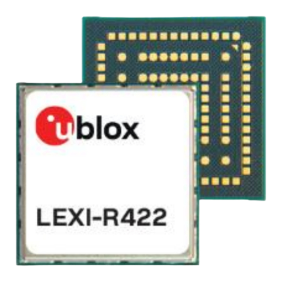
LEXI-R422
Ultra-small LTE-M / NB-IoT / EGPRS module
System integration manual
Abstract
This document describes the features and the integration of the ultra-small LEXI-R422 cellular
modules. These modules are a complete, cost efficient, performance optimized, multi-mode and
multi-band LTE-M / NB-IoT / EGPRS solution in the compact LEXI form factor.
UBX-23007449 - R02
C1-Public
www.u-blox.com
Advertisement
Table of Contents

Related Manuals for u-blox LEXI-R422


Summary of Contents for u-blox LEXI-R422
- Page 1 System integration manual Abstract This document describes the features and the integration of the ultra-small LEXI-R422 cellular modules. These modules are a complete, cost efficient, performance optimized, multi-mode and multi-band LTE-M / NB-IoT / EGPRS solution in the compact LEXI form factor.
-
Page 2: Document Information
The information contained herein is provided “as is” and u-blox assumes no liability for its use. No warranty, either express or implied, is given, including but not limited to, with respect to the accuracy, correctness, reliability and fitness for a particular purpose of the information. -
Page 3: Table Of Contents
LEXI-R422 - System integration manual Contents Document information ..........................2 Contents ................................3 System description ..........................6 1.1 Overview ................................ 6 1.2 Architecture ..............................8 1.3 Pin-out ................................9 1.4 Operating modes ............................12 1.5 Supply interfaces ............................. 15 1.5.1 Module supply input (VCC) ......................15 1.5.2 Generic digital interfaces supply output (V_INT) .............. - Page 4 2.9 Module placement ........................... 81 2.10 Module footprint and paste mask ......................82 2.11 Thermal guidelines ..........................83 2.12 Schematic for LEXI-R422 modules integration ................. 84 2.13 Design-in checklist ........................... 85 2.13.1 Schematic checklist ........................85 2.13.2 Layout checklist ..........................85 2.13.3 Antenna checklist ..........................
- Page 5 Product testing............................ 99 5.1 Validation testing and qualification ..................... 99 5.2 Production testing ..........................100 5.2.1 u-blox in-line production tests ....................100 5.2.2 Production test parameters for OEM manufacturers ............100 Appendix ..............................102 Migration from SARA-R42 series modules ................102 Glossary ...............................
-
Page 6: System Description
LEXI-R422 - System integration manual System description 1.1 Overview The LEXI-R422 modules are a multi-band LTE-M / NB-IoT / EGPRS multi-mode solution in the ultra-small LEXI LGA form factor (16.0 x 16.0 mm, 133-pin), allowing an easy integration into compact designs. - Page 7 236.8 kb/s UL up to 296 kb/s DL Table 2: LEXI-R422 modules cellular characteristics summary GPRS/EGPRS multi-slot cass 33 implies a maximum of 5 slots in Down-Link and 4 slots in Up-Link with 6 slots in total. UBX-23007449 - R02...
-
Page 8: Architecture
V_INT Management PWR_CTRL Figure 1: LEXI-R422 modules’ simplified block diagram Below is a detailed description of LEXI-R422 modules sections shown in figure above. Cellular RF section The cellular RF section is composed of the following main elements: • RF switch connecting the antenna port (ANT) to the suitable RF Tx / Rx paths •... -
Page 9: Pin-Out
LEXI-R422 - System integration manual 1.3 Pin-out Table 3 lists the pin-out of the LEXI-R422 modules, with pins grouped by function. Function Name I/O Description Remarks Power 40-42 A12-14 Module supply VCC supply circuit affects the RF performance and input compliance of the device integrating the module with applicable required certification schemes. - Page 10 LEXI-R422 - System integration manual Function Name I/O Description Remarks UART UART data Primary UART circuit 104 (RxD) in ITU-T V.24, output for AT commands, data, Mux, FOAT. See section 1.9.1 for functional description. See section 2.6.1 for external circuit design-in.
- Page 11 72,80,81, F5,G3,G5, 89,90,98, H3,H5,J3, 107,108 K3,K5 RSVD N/A Reserved pin Provide test point for diagnostic purposes. See sections 1.12 and 2.8. Table 3: LEXI-R422 modules pin definition, grouped by function UBX-23007449 - R02 System description Page 11 of 108 C1-Public...
-
Page 12: Operating Modes
LEXI-R422 - System integration manual 1.4 Operating modes LEXI-R422 modules have several operating modes. The operating modes are defined in Table 4 described in detail in Table 5, providing general guidelines for operation. General status Operating mode Definition Power-down Not-powered mode VCC supply not present or below operating range: module is switched off. - Page 13 RF Tx/Rx activity is necessary. When a data connection is terminated, the module returns to the active mode. Table 5: LEXI-R422 modules operating modes description UBX-23007449 - R02 System description Page 13 of 108...
- Page 14 LEXI-R422 - System integration manual The initial operating mode of LEXI-R422 modules is the one with VCC supply not present or below the operating range: the modules are switched off in not-powered mode. Once a valid VCC supply is applied to the LEXI-R422 modules, they remain switched off in the power-off mode.
-
Page 15: Supply Interfaces
Tx / Rx call at maximum RF power level (see the LEXI-R422 data sheet [1]). LEXI-R422 modules, supporting 2G radio access technology, provide separate supply inputs over the three VCC pins: •... - Page 16 VCC supply circuit compliant with the requirements listed in Table ⚠ The supply circuit affects the RF compliance of the device integrating LEXI-R422 modules with applicable required certification schemes as well as antenna circuit design. RF performance is optimized by fulfilling the requirements summarized in the...
- Page 17 (approximately 2 W or 33 dBm in the Tx slot/burst), then the current consumption can reach a high peak / pulse (see the LEXI-R422 data sheet [1]) for 576.9 µs (width of the transmit slot/burst) with a periodicity of 4.615 ms (width of 1 frame = 8 slots/burst), that is, with a 1/8 duty cycle according to GSM TDMA (Time Division Multiple Access).
- Page 18 LEXI-R422 - System integration manual Figure 5 shows an example of the module current consumption profile versus time in 2G single-slot. Current [A] 1 900 mA 1 .5 Peak current depends on TX power and 1 .0 actual antenna load...
- Page 19 When PSM is enabled, the module automatically enters the PSM and the ultra-low power deep-sleep mode whenever possible. LEXI-R422 modules may automatically enter the ultra-low power deep-sleep mode in-between eDRX cycles, whenever possible, if the functionality is enabled by the +UPSMVER AT command, see the AT commands manual and the application development guide [3].
- Page 20 (DRX) mode. See detailed current consumption values in the LEXI-R422 data sheet [1]. Current [mA] Time [s]...
-
Page 21: Generic Digital Interfaces Supply Output (V_Int)
The typical operating voltage is 1.8 V, whereas the current capability is specified in the LEXI-R422 data sheet [1]. The V_INT voltage domain can be used in place of an external discrete regulator as a reference voltage rail for external components. -
Page 22: System Function Interfaces
1.6 System function interfaces 1.6.1 Module power-on When the LEXI-R422 modules are in the not-powered mode (i.e. the VCC module supply is not applied), they can be switched on as follows: • Rising edge on the VCC input pins to a valid voltage level, and then a low logic level needs to be set at the PWR_CTRL input pin for a valid time When the LEXI-R422 modules are in the power-off mode (i.e. -
Page 23: Module Power-Off
• AT+CPWROFF command (see AT commands manual [2]) • Low pulse on the PWR_CTRL pin for a valid time period (for detailed characteristics, see LEXI-R422 data sheet [1]) ☞ The graceful shutdown must be started as indicated above, and then a proper VCC supply must be held at least until the end of the modules’... - Page 24 • When the +CPWROFF AT command is sent, or when a low pulse is applied at the PWR_CTRL input pin with appropriate time duration (see the LEXI-R422 data sheet [1]), the module starts the switch-off routine. • Then, if the +CPWROFF AT command has been sent, the module replies OK on the AT interface: the switch-off routine is in progress.
-
Page 25: Module Reset
An abrupt hardware reset (reboot) occurs on the LEXI-R422 modules when a low level is applied on PWR_CTRL input pin for a long time period (see the LEXI-R422 data sheet [1]). In this case, the current parameter settings are not saved in the module’s non-volatile memory and a clean network detach is not performed. -
Page 26: Antenna Interfaces
1.7.1 Cellular antenna RF interface (ANT) LEXI-R422 modules provide an RF interface for connecting the external cellular antenna. The ANT pin represents the primary RF input/output for transmission and reception of cellular RF signals. The ANT pin has a nominal characteristic impedance of 50 and must be connected to the cellular Tx / Rx antenna system through a 50 ... -
Page 27: Antenna Detection Interface (Ant_Det)
1.8 SIM interface 1.8.1 SIM interface LEXI-R422 modules provide a SIM interface on the VSIM, SIM_IO, SIM_CLK, SIM_RST pins to connect an external SIM card or UICC chip. LEXI-R422 modules support only the 1.8 V type of SIM / UICC. -
Page 28: Uart Interfaces
Modem status and control lines (DTR input, DSR output, DCD output, RI output) ☞ UART signal names of LEXI-R422 modules conform to the ITU-T V.24 [5]: e.g. TXD line represents data transmitted by the DTE (host processor output) and received by the DCE (module input). -
Page 29: Usb Interface
LEXI-R422 modules include a high-speed USB 2.0 interface [4], available for FW upgrade by means of the u-blox EasyFlash tool and for diagnostic purposes. The module itself acts as a USB device, and it can be connected to a USB host such as a Personal Computer equipped with compatible drivers. -
Page 30: General Purpose Input / Output
LEXI-R422 - System integration manual 1.10 General purpose input / output LEXI-R422 modules include pins which can be configured as general purpose input/output or to provide custom functions via u-blox AT commands (for details, see the AT commands manual [2],... -
Page 31: Reserved Pins (Rsvd)
LEXI-R422 - System integration manual 1.12 Reserved pins (RSVD) LEXI-R422 modules have pins reserved for future use, marked as RSVD, which can all be left unconnected on the application board, except for the RSVD #99 (J5) pin which is recommended to be externally accessible by connecting it to a dedicated Test-Point. -
Page 32: Design-In
LEXI-R422 - System integration manual Design-in 2.1 Overview For an optimal integration of the LEXI-R422 modules in the final application board, follow the design guidelines stated in this section. Every application circuit must be suitably designed to ensure the correct functionality of the relative interface, but a number of points require greater attention during the design of the application device. -
Page 33: Supply Interfaces
The switching step-down regulator is the typical choice when primary supply source has a nominal voltage much higher (e.g. greater than 5 V) than the operating supply voltage of LEXI-R422. The use of switching step-down provides the best power efficiency for the overall application and minimizes current drawn from the main supply source. - Page 34 The selected regulator or battery must be able to support with adequate margin the highest averaged current consumption value specified in the LEXI-R422 data sheet [1]. The following sections highlight some design aspects for each of the supplies listed above providing...
- Page 35 LEXI-R422 modules, where the module VCC input is supplied by a step-down switching regulator capable of delivering the highest peak / pulse current specified for the 2G use-case, with low output ripple and with fixed switching frequency in PWM mode operation greater than 1 MHz.
- Page 36 A1 3 A1 4 C1 0 SYNC COMP Figure 18: Example of low cost VCC supply circuit for LEXI-R422 modules, using a step-down regulator Reference Description Part number - Manufacturer 22 µF capacitor ceramic X5R 1210 10% 25 V Generic manufacturer...
- Page 37 LEXI-R422 A1 2 A1 3 A1 4 SHDN Figure 19: Example of high reliability VCC supply circuit for LEXI-R422 modules, using an LDO linear regulator Reference Description Part number - Manufacturer 10 µF capacitor ceramic X5R 0603 20% 6.3 V Generic manufacturer 100 µF capacitor tantalum B_SIZE 20% 6.3V 15m...
- Page 38 Generic manufacturer LDO linear regulator ADJ 3.0 A LP38501ATJ-ADJ/NOPB - Texas Instrument Table 13: Suggested components for low cost VCC supply circuit for LEXI-R422 modules, using an LDO linear regulator ☞ See the section 2.2.1.10, and in particular Figure 26...
- Page 39 VCC pins must be capable of delivering the maximum current occurring during a transmission at maximum Tx power, as specified in the LEXI-R422 data sheet [1]. The maximum discharge current is not always reported in the data sheets of batteries, but the maximum DC discharge current is typically almost equal to the battery capacity in Amp-hours divided by 1 hour.
- Page 40 LEXI-R422 - System integration manual The battery charger IC, as linear charger, is more suitable for applications where the charging source has a relatively low nominal voltage (~5 V), so that a switching charger is suggested for applications where the charging source has a relatively high nominal voltage (e.g. ~12 V, see section 2.2.1.7...
- Page 41 LEXI-R422 - System integration manual A power management IC should meet the following prerequisites to comply with the module VCC requirements summarized in Table • High efficiency internal step down converter, with characteristics as indicated in section 2.2.1.2 • Low internal resistance in the active path Vout – Vbat, typically lower than 50 m...
- Page 42 LEXI-R422 - System integration manual Using a battery pack with an internal NTC resistor, the MP2617H can monitor the battery temperature to protect the battery from operating under unsafe thermal conditions. Several parameters as the charging current, the charging timings, the input current limit, the input...
- Page 43 412 k resistor 0402 5% 0.063 W Step-up regulator 350 mA AP3015 - Diodes Incorporated Table 16: Examples of parts for the VCC circuit with separate supply for LEXI-R422 modules ☞ See the section 2.2.1.10, and in particular Figure 26...
- Page 44 VCC power is in general not strictly needed, but it may be useful to further minimize the current consumption when the LEXI-R422 modules are switched off. The VCC supply source can be removed using an appropriate low-leakage load switch or p-channel...
- Page 45 LEXI-R422 - System integration manual 2.2.1.10 Additional guidelines for VCC supply circuit design To reduce voltage drops, use a low impedance power source. The series resistance of the supply lines (connected to the modules VCC and GND pins) on the application board and battery pack should also be considered and minimized: cabling and routing must be as short as possible to minimize losses.
- Page 46 RF signal; this is more likely to happen with switching DC-DC converters, in which case it is better to select the highest operating frequency for the switcher and add a large L-C filter before connecting to the LEXI-R422 modules in the worst case.
-
Page 47: Generic Digital Interfaces Supply Output (V_Int)
Generic digital interfaces supply output (V_INT) 2.2.2.1 Guidelines for V_INT circuit design LEXI-R422 modules provide the V_INT generic digital interfaces 1.8 V supply output, which can be mainly used to: • Indicate when the module is switched on and it is not in the deep-sleep power saving mode (as described in sections 1.6.1, 1.6.2) -
Page 48: System Functions Interfaces
The PWR_CTRL circuit requires careful layout since it is the sensitive input available to switch on and switch off the LEXI-R422 modules. It is required to ensure that the voltage level is well defined during operation and no transient noise is coupled on this line, otherwise the module might detect a spurious power-on request. -
Page 49: Antenna Interfaces
LEXI-R422 - System integration manual 2.4 Antenna interfaces LEXI-R422 modules provide an RF interface for connecting the external antenna: the ANT pin represents the RF input/output for RF signals transmission and reception. The ANT pin has a nominal characteristic impedance of 50 and must be connected to the related external antenna system through a 50 ... - Page 50 LEXI-R422 - System integration manual 500 µm 380 µm 500 µm L1 copper 35 µm FR-4 dielectric 270 µm L2 copper 35 µm FR-4 dielectric 760 µm L3 copper 35 µm FR-4 dielectric 270 µm L4 copper 35 µm Figure 30: Example of 50 coplanar waveguide transmission line design for the described 4-layer board layup 400 µm...
- Page 51 See section 2.4.1.6 for the description of the antenna trace design implemented on the u-blox host printed circuit board used for conformity assessment of LEXI-R422 surface-mounted modules for regulatory type approvals such as FCC United States, ISED Canada, RED Europe, etc.
- Page 52 See section 2.4.1.6 for the description of the antenna trace design implemented on the u-blox host printed circuit board used for conformity assessment of LEXI-R422 surface-mounted modules for regulatory type approvals such as FCC United States, ISED Canada, RED Europe, etc.
- Page 53 LEXI-R422 - System integration manual • External antennas (e.g. linear monopole): External antennas basically do not imply physical restriction to the design of the PCB where the LEXI-R422 module is mounted. The radiation performance mainly depends on the antennas: it is required to select antennas with optimal radiating performance in the operating bands.
- Page 54 LEXI-R422 - System integration manual 2.4.1.5 Examples of cellular antennas Table 20 lists some examples of possible internal on-board surface-mount antennas. Manufacturer Part number Product name Description Taoglas PA.710.A Warrior GSM / WCDMA / LTE SMD antenna 698..960 MHz, 1710..2170 MHz, 2300..2400 MHz, 2490..2690 MHz...
- Page 55 LEXI-R422 - System integration manual Table 21 lists some examples of possible internal off-board PCB-type antennas with cable and connector. Manufacturer Part number Product name Description PulseLarsen W3929B0100 LTE FPC antenna with coax feed Antennas 617..960 MHz, 1710..2690 MHz, 3400..3900 MHz 115.8 x 30.4 mm...
- Page 56 FCC United States, ISED Canada, RED Europe, etc. has been carried out with the modules mounted on a u-blox host printed circuit board (PCB) with a 50 grounded coplanar waveguide designed on it, herein referenced as “antenna trace design”. The antenna trace design implements the connection of the ANT LGA pad of the module, which is the cellular RF input/output of the module, up to a dedicated 50 ...
- Page 57 SMA6251A1-3GT50G-50 – Amphenol Table 23: Parts in use on the u-blox host PCB for the antenna trace design, with additional antenna detection circuit The u-blox host PCB has a structure of 6 copper layers with 35 µm thickness (1 oz/ft ) for all the layers except the two inner buried layers, having 18 µm thickness (1/2 oz/ft...
- Page 58 RF trace as illustrated in Figure Figure 37: Buried metal layer (L2) layout of the u-blox host PCB, below the antenna RF trace design Guidelines to design an equivalent proper connection for the ANT pad are available in section 2.4.1.1.
-
Page 59: Cellular And Gnss Rf Coexistence
LEXI-R422 - System integration manual 2.4.2 Cellular and GNSS RF coexistence Overview Desensitization or receiver blocking is a form of electromagnetic interference where a radio receiver is unable to detect a weak signal that it might otherwise be able to receive when there is no... - Page 60 LEXI-R422 - System integration manual Out-of-band interference Out-of-band interference is caused by signal frequencies that are different from the GNSS, the main sources being cellular, Wi-Fi, bluetooth transmitters, etc. For example, the lowest channels in LTE band 3, 4 and 66 can compromise the good reception of the GLONASS satellites. Again, the effect can be explained by comparing the LTE frequencies (low channel transmission frequency is 1710 MHz) with the GLONASS operating band (1602 MHz ±...
-
Page 61: Antenna Detection Interface (Ant_Det)
5.5 cm SARA GNSS module antenna Cellular antenna Figure 39: PCB top rendering for the u-blox B36 blueprint with annotated distance between cellular and GNSS antennas 2.4.3 Antenna detection interface (ANT_DET) 2.4.3.1 Guidelines for ANT_DET circuit design Figure 40 Table 25... - Page 62 LEXI-R422 - System integration manual The antenna detection circuit and diagnostic circuit suggested in Figure 40 Table 25 are here explained: • When antenna detection is forced by the +UANTR AT command, the ANT_DET pin generates a DC current measuring the resistance (R2) from the antenna connector (J1) provided on the application board to GND.
-
Page 63: Cellular Antenna Dynamic Tuner Interface
2.4.4 Cellular antenna dynamic tuner interface LEXI-R422 modules include two output pins (named RFCTRL1 and RFCTRL2) that can be configured, as optional feature, to change their output value dynamically according to the specific actual cellular band in use by the module. These pins, paired with an external antenna tuner IC or RF switch, can be used to: •... - Page 64 42(a), tuning the antenna impedance optimizes the power delivered into the antenna by dynamically adjusting the RF impedance seen by ANT pin of LEXI-R422 module. By creating a tuned matching network for each operating band, the total radiated power (TRP) and the total isotropic sensitivity (TIS) metrics are improved.
-
Page 65: Sim Interface
LEXI-R422 - System integration manual 2.5 SIM interface 2.5.1 Guidelines for SIM circuit design 2.5.1.1 Guidelines for SIM cards, SIM connectors and SIM chips selection The ISO/IEC 7816, the ETSI TS 102 221 and the ETSI TS 102 671 specifications define the physical,... - Page 66 LEXI-R422 - System integration manual 2.5.1.2 Guidelines for single SIM card connection without detection A removable SIM card placed in a SIM card holder must be connected to the SIM card interface of LEXI-R422 modules as described in Figure 43, where the optional SIM detection feature is not implemented.
- Page 67 Guidelines for single SIM chip connection A Surface-Mounted SIM chip (M2M UICC Form Factor) must be connected the SIM card interface of the LEXI-R422 modules as described in Figure Follow these guidelines to connect the module to a Surface-Mounted SIM chip without SIM presence detection: •...
- Page 68 LEXI-R422 - System integration manual • Connect one pin of the normally-open mechanical switch integrated in the SIM connector (as the SW2 pin in Figure 45) to the GPIO6 input pin, providing a weak pull-down resistor (e.g. 470 k, as...
-
Page 69: Guidelines For Sim Layout Design
The layout of the SIM card interface lines (VSIM, SIM_CLK, SIM_IO, SIM_RST) may be critical if the SIM card is placed far away from the LEXI-R422 modules or in close proximity to the RF antenna: these two cases should be avoided or at least mitigated as described below. -
Page 70: Data Communication Interfaces
LEXI-R422 - System integration manual 2.6 Data communication interfaces 2.6.1 UART interfaces 2.6.1.1 Guidelines for UART circuit design Providing 1 UART with full RS-232 functionality (using the complete V.24 link) If RS-232 compatible signal levels are needed, two different external voltage translators can be used to provide full RS-232 (9 lines) functionality: e.g. - Page 71 LEXI-R422 - System integration manual Providing 1 UART with TXD, RXD, RTS, CTS and DTR lines only If the functionality of the DSR, DCD and RI lines is not required, or the lines are not available: • Leave DSR, DCD and RI lines of the module floating If RS-232 compatible signal levels are needed, two different external voltage translators (e.g.
- Page 72 LEXI-R422 - System integration manual Providing 1 UART with TXD, RXD, RTS and CTS lines only If the functionality of the DSR, DCD, RI and DTR lines is not required, or the lines are not available: • Connect the module DTR input to GND using a 0 series resistor, since it may be useful to set...
- Page 73 Providing 2 UARTs with the TXD, RXD, RTS and CTS lines LEXI-R422 modules include an auxiliary UART interface (UART AUX), as alternative mutually exclusive function over the DTR, DSR, DCD and RI pins, with settings configurable by dedicated AT commands (see the AT commands manual [2]): •...
- Page 74 LEXI-R422 - System integration manual Providing 1 UART with TXD and RXD lines only ☞ Providing the TXD and RXD lines only is not recommended if the multiplexer functionality is used in the application: providing also at least the HW flow control (RTS and CTS lines) is recommended, and it is in paricular necessary if the low power mode is enabled by +UPSV AT command.
-
Page 75: Usb Interface
LEXI-R422 - System integration manual Additional considerations If a 3.0 V Application Processor (DTE) is used, the voltage scaling from any 3.0 V output of the DTE to the corresponding 1.8 V input of the module (DCE) can be implemented as an alternative low-cost solution, by means of an appropriate voltage divider. - Page 76 LEXI-R422 - System integration manual The LEXI-R422 modules do not support AT command / data communication over USB interface: the USB interface is available on these modules product versions for FW upgrade by means of the dedicated u-blox EasyFlash tool and for diagnostic purposes only. Therefore, the USB interface of these modules product versions is not designed to be connected to an external host processor mounted on the application board.
- Page 77 LEXI-R422 - System integration manual 2.6.2.2 Guidelines for USB layout design The USB_D+ / USB_D- lines require accurate layout design to achieve reliable signaling at the high speed data rate (up to 480 Mb/s) supported by the USB serial interface.
-
Page 78: I2C Interface
GNSS receiver: • The SDA and SCL pins of the cellular module are directly connected to the related pins of the u-blox 1.8 V GNSS receiver. External pull-up resistors are not needed, as they are already integrated in the cellular module. - Page 79 • The GPIO3 pin is connected to the TxD pin of the u-blox 3.0 V GNSS receiver providing the additional “GNSS Tx data ready” function, using a suitable unidirectional general purpose voltage translator (e.g. TI SN74AVC2T245, which additionally provides the partial power down feature so that the 3.0 V GNSS supply can be also ramped up before the V_INT 1.8 V cellular supply.
-
Page 80: General Purpose Input / Output
2.7 General purpose input / output 2.7.1 Guidelines for GPIO circuit design A typical usage of LEXI-R422 modules GPIOs can be the following: • Network indication provided over GPIO1 pin (see Figure 61... -
Page 81: Reserved Pins (Rsvd)
LEXI-R422 - System integration manual 2.8 Reserved pins (RSVD) LEXI-R422 modules have pins reserved for future use, marked as RSVD, which can all be left unconnected on the application board, except for the RSVD pin number 99 (also identified as J5), which is recommended to be externally accessible by connecting it to a dedicated Test-Point. -
Page 82: Module Footprint And Paste Mask
16.0 All dimensions in millimeters Figure 63: Suggested footprint and paste mask for LEXI-R422 modules (application board top view) ☞ These are recommendations only and not specifications. The exact copper, solder and paste mask geometries, distances, stencil thicknesses and solder paste volumes must be adapted to the specific production processes (e.g. -
Page 83: Thermal Guidelines
Document [10]); however the application should be correctly designed to cope with it. During transmission at maximum RF power the LEXI-R422 modules generate thermal power that may exceed 0.5 W: this is an indicative value since the exact generated power strictly depends on operating condition such as the actual antenna return loss, the transmitting frequency band, etc. -
Page 84: Schematic For Lexi-R422 Modules Integration
LEXI-R422 - System integration manual 2.12 Schematic for LEXI-R422 modules integration Figure 64 is an example of a schematic diagram where a LEXI-R422 module is integrated into an application board using almost all available interfaces and functions. LEXI-R422 Cellular antenna... -
Page 85: Design-In Checklist
Provide adequate precautions for EMC / ESD immunity as required on the application board. Do not apply voltage to any generic digital interface pin of LEXI-R422 modules before the switch-on of the generic digital interface supply source (V_INT). ... -
Page 86: Antenna Checklist
LEXI-R422 - System integration manual Route VCC supply line away from RF line / part (refer to Figure 27) and other sensitive analog lines / parts. The VCC bypass capacitors in the picoFarad range should be placed as close as possible to the VCC pins, in particular if the application device integrates an internal antenna. -
Page 87: Handling And Soldering
The term is usually used in the electronics and other industries to describe momentary unwanted currents that may cause damage to electronic equipment. The ESD sensitivity for each pin of LEXI-R422 modules (considering the Human Body Model according to JS-001-2017 and the Charged Device Model according to JS-002-2018) is specified in LEXI-R422 data sheet [1]. -
Page 88: Soldering
3.3 Soldering 3.3.1 Soldering paste "No Clean" soldering paste is strongly recommended for LEXI-R422 modules, as it does not require cleaning after the soldering process has taken place. The paste listed in the example below meets these criteria. Soldering Paste: OM338 SAC405 / Nr.143714 (Cookson Electronics) -
Page 89: Optical Inspection
LEXI-R422 - System integration manual Cooling phase A controlled cooling avoids negative metallurgical effects (solder becomes more brittle) of the solder and possible mechanical tensions in the products. Controlled cooling helps to achieve bright solder fillets with a good shape and low contact angle. -
Page 90: Repeated Reflow Soldering
Boards with combined through-hole technology (THT) components and surface-mount technology (SMT) devices require wave soldering to solder the THT components. No more than one wave soldering process is allowed for a board with a LEXI-R422 module already populated on it. ⚠... -
Page 91: Grounding Metal Covers
☞ u-blox gives no warranty for damages to the cellular modules caused by soldering metal cables or any other forms of metal strips directly onto the EMI covers. 3.3.12 Use of ultrasonic processes The cellular modules contain components which are sensitive to ultrasonic waves. -
Page 92: Approvals
The required certification scheme approvals and relative testing specifications applicable to the end-device that integrates a LEXI-R422 module differ depending on the country or the region where the integrating device is intended to be deployed, on the relative vertical market of the device, on type, features and functionalities of the whole application device, and on the network operators where the device is intended to operate. -
Page 93: Federal Communications Commission Notice
Table 39: List of FCC / ISED rules applicable to LEXI-R422 modules The LEXI-R422 modular transmitter is only FCC authorized for the specific rule parts listed on the FCC grant. The host product manufacturer is responsible for compliance to any other FCC rules that apply to the host not covered by the modular transmitter grant of certification. - Page 94 RF exposure or any other. 4.2.1.7 Label and compliance information If the FCC Grant of the LEXI-R422 modular transmitter can be used for the final host product, as the conditions referenced in the certificates and in this chapter 4.2.1...
-
Page 95: Innovation, Science, Economic Development Canada Notice
4.2.1.9 Additional testing, Part 15 Subpart B disclaimer LEXI-R422 modular transmitter is only FCC authorized for the specific rule parts listed on the FCC grant (see section 4.2.1.1). The host product manufacturer is responsible for compliance to any other FCC rules that apply to the host not covered by the modular transmitter grant of certification. -
Page 96: Modifications
Modifications ISED Canada requires the user to be notified that any changes or modifications made to this device that are not expressly approved by u-blox could void the user's authority to operate the equipment. ⚠ Manufacturers of mobile or fixed devices incorporating the LEXI-R422 modules are authorized to use the ISED Canada Certificates of the LEXI-R422 modules for their own final products according to the conditions referenced in the certificates. -
Page 97: European Conformance Ce Mark
⚠ The gain of the system antenna(s) used for LEXI-R422 modules (i.e. the combined transmission line, connector, cable losses and radiating element gain) must not exceed the values reported in the Declaration of Conformity, for mobile and fixed or mobile operating configurations The conformity assessment procedure for the LEXI-R422 modules, referred to in Article 17 and detailed in Annex II of Directive 2014/53/EU, has been followed. -
Page 98: Conformity Assessed (Ukca)
⚠ The gain of the system antenna(s) used for LEXI-R422 modules (i.e. the combined transmission line, connector, cable losses and radiating element gain) must not exceed the values reported in the Declaration of Conformity, for mobile and fixed or mobile operating configurations The conformity assessment procedure for the modules, referred to Part 3 of the Radio Equipment Regulations 2017, has been followed. -
Page 99: Product Testing
The 50 characteristic impedance of the antenna trace design on a host printed circuit board can be verified using a Vector Network Analyzer, as done on the u-blox host PCB, with calibrated RF coaxial cable soldered at the pad corresponding to RF input/output of the module and with the transmission line terminated to a 50 ... -
Page 100: Production Testing
5.2.1 u-blox in-line production tests u-blox focuses on high quality for its products. All units produced are tested automatically in all their interfaces along the production line. Stringent quality control processes have been implemented in the production line. Defective units are analyzed in detail to improve production quality. - Page 101 Communication with external I2C devices can be checked using dedicated I2C AT commands • GPIO functionality can be checked using the dedicated +UGPIOC AT command, etc. Please contact the u-blox office or sales representative nearest you for further guidelines about OEM production testing guidelines. 5.2.2.1 “Go/No go”...
-
Page 102: Appendix
SARA-R42 series modules (26 x 16 mm, 96-pin LGA), consisting of the SARA-R422, SARA-R422S, SARA-R422M8S and SARA-R422M10S modules, and LEXI-R422 modules (16 x 16 mm, 133-pin LGA) have a different form-factor, but they integrate the same key internal components, offering the same electrical characteristics and allowing the use of the same external circuits. - Page 103 Several ground pins are available with LEXI-R422 modules Several ground pins are available with LEXI-R422 modules Table 40: Pin assignment of SARA-R42 series and LEXI-R422 modules, with remarks for migration ☞ For more information about SARA-R42 series modules, see the SARA-R4 series data sheet [18], the SARA-R4 series system integration manual [19], and the AT commands manual [2].
-
Page 104: B Glossary
LEXI-R422 - System integration manual Glossary Abbreviation Definition Generation Cellular Technology (GSM, GPRS, EGPRS) Generation Cellular Technology (UMTS, HSDPA, HSUPA) 3GPP Generation Partnership Project ACMA Australian Communications and Media Authority Analog to Digital Converter ANATEL Agência Nacional de Telecomunicações – National Telecommunications Agency (Brazil) - Page 105 Message Queuing Telemetry Transport Not Applicable Non-Access Stratum National Communications Commission Taiwan Original Equipment Manufacturer device: an application device integrating a u-blox cellular module Over The Air Power Amplifier Product Change Notification / Sample Delivery Note / Information Note Pulse Frequency Modulation...
- Page 106 LEXI-R422 - System integration manual Abbreviation Definition Total Radiated Power UART Universal Asynchronous Receiver-Transmitter User Datagram Protocol User Equipment UICC Universal Integrated Circuit Card UKCA United Kingdom Conformity Assessed Up-Link (Transmission) UMTS Universal Mobile Telecommunications System United States Universal Serial Bus...
-
Page 107: Related Documentation
UBX-20012630 [18] u-blox SARA-R4 series data sheet, UBX-16024152 [19] u-blox SARA-R4 series system integration manual, UBX-16029218 ☞ For regular updates to u-blox documentation and to receive product change notifications, register on our homepage (www.u-blox.com). Revision history Revision Date Name Comments... -
Page 108: Contact
LEXI-R422 - System integration manual Contact u-blox AG Address: Zürcherstrasse 68 8800 Thalwil Switzerland For further support and contact information, visit us at www.u-blox.com/support. UBX-23007449 - R02 Contact Page 108 of 108 C1-Public...
Need help?
Do you have a question about the LEXI-R422 and is the answer not in the manual?
Questions and answers