Table of Contents
Advertisement
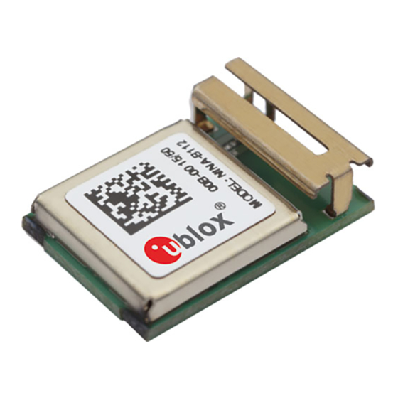
NINA-B1 series
Stand-alone Bluetooth low energy
modules
System Integration Manual
Abstract
This document describes the system integration of NINA-B1 series
®
stand-alone Bluetooth
low energy modules.
Bluetooth low energy stack and u-blox connectivity software, these
modules are tailored for OEMs who wish to have the shortest time-
to-market. The OEMs can also embed their own application on top
of the integrated Bluetooth low energy stack using Nordic SDK or
®
Arm
Mbed™ integrated development environment (IDE).
www.u-blox.com
UBX-15026175 - R09
With embedded
Advertisement
Table of Contents

Related Manuals for u-blox NINA-B112


Summary of Contents for u-blox NINA-B112
- Page 1 Bluetooth low energy modules. With embedded Bluetooth low energy stack and u-blox connectivity software, these modules are tailored for OEMs who wish to have the shortest time- to-market. The OEMs can also embed their own application on top of the integrated Bluetooth low energy stack using Nordic SDK or ®...
-
Page 2: U-Blox Reserves All Rights To This Document And The Information Contained Herein. Products, Names, Logos And Designs Described Herein May In
This document may be revised by u-blox at any time. For most recent documents, visit www.u-blox.com. Copyright © 2017, u-blox AG. u-blox is a registered trademark of u-blox Holding AG in the EU and other countries. Arm is a registered trademark of Arm Limited (or its subsidiaries) in the US and/or elsewhere. -
Page 3: Table Of Contents
1.7.1 Analog interfaces ........................13 Antenna interfaces ..........................14 1.8.1 Antenna pin – NINA-B111 ......................14 1.8.2 Integrated antenna – NINA-B112....................15 1.8.3 NFC antenna ..........................15 Reserved pins (RSVD) .......................... 15 1.10 GND pins ............................15 Software ........................16 u-blox connectivity software ....................... - Page 4 3.2.1 RF transmission line design (NINA-B111 only) ................28 3.2.2 Antenna design (NINA-B111 only) ....................30 3.2.3 On-board antenna design (NINA-B112 only) ................32 Supply interfaces ..........................33 3.3.1 Module supply design ......................... 33 Data communication interfaces ......................33 3.4.1 Asynchronous serial interface (UART) design ................
-
Page 5: System Description
NINA-B112 comes with an internal antenna and NINA-B111 has a pin for use with an external antenna. The internal PIFA antenna is specifically designed for the small NINA-B1 form factor and provides an extensive range of more than 300 m, independent of ground plane and component placement. -
Page 6: Module Architecture
1.1.3 Software options The NINA-B1 series module can be used either together with the pre-flashed u-blox connectivity software or as an Open CPU module where you can run your own application developed with either Arm Mbed, Nordic SDK or Wirepas development environment inside the NINA-B1 module. -
Page 7: Pin Description
The grey pins in the center of the modules are GND pins. The outline of NINA-B111 ends at the dotted line as shown in Figure 2, where the antenna area of NINA-B112 begins. All digital or analog functions described in this manual can be freely assigned to any GPIO pin. Analog functions are limited to analog capable pins. -
Page 8: Ubx-15026175 - R09
NINA-B1 series - System Integration Manual Do not apply an NFC field to the NFC pins when they are configured as GPIOs. Doing so may cause permanent damage to the module. When driving different logic levels on these pins in GPIO mode, a small current leakage will occur, make sure they are set to the same logic level before entering into any power saving modes. -
Page 9: Ubx-15026175 - R09
Grounding SWITCH_2 during reset will reset the UART serial settings. • Can be use as external connect or to enable parable mode. See u-blox Short Range Modules AT Commands Manual [4] for more details. GPIO_20 P0.31 General purpose I/O UART_RTS:... -
Page 10: Supply Interfaces
15 mA Table 3: Summary of voltage supply requirements The current requirement in Table 3 considers using the u-blox connectivity software with UART comunication. But it does not include any aditional I/O current. Any use of external push-buttons, LEDs, or other interfaces will add to the total current consumption of the NINA-B1 module. -
Page 11: Digital I/O Interfaces Reference Voltage (Vcc_Io)
NINA-B1 series - System Integration Manual 1.3.2 Digital I/O interfaces reference voltage (VCC_IO) On the NINA-B1 series modules, the I/O voltage level is the same as the supply voltage and VCC_IO is internally connected to the supply input VCC. When using NINA-B1 with a battery, the I/O voltage level will vary with the battery output voltage, depending on the charge of the battery. -
Page 12: Serial Interfaces
The u-blox connectivity software adds the DSR and DTR pins to the UART interface. These pins are not used as originally intended, but to control the state of the NINA-B1 module. Depending on the current configuration, the DSR can be used to: •... -
Page 13: Gpio Pins
BLUE** indication * = If left unconfigured ** = If using u-blox connectivity software Table 5: GPIO custom functions configuration 1.7.1 Analog interfaces 8 out of the 19 digital GPIOs can be multiplexed to analog functions. The following analog functions are available for use: •... -
Page 14: Antenna Interfaces
NINA-B1 series - System Integration Manual ACQ [us] Maximum source resistance [kΩ] Table 6: Acquisition vs source impedance 1.7.1.2 Comparator The comparator compares voltages from any analog pin with different references as shown in Table 7. It supports full 0 V to VCC input range and can generate different software events to the rest of the system. 1.7.1.3 Low power comparator The low-power comparator operates in the same way as the normal comparator, with reduced functionality. -
Page 15: Integrated Antenna - Nina-B112
The NINA-B112 is equipped with an integrated antenna on the module. This will simplify the integration as there will be no need to do RF trace design on the host PCB. By using the NINA-B112 with integrated antenna, the certification of the NINA-B1 series module can be reused, thus minimizing the effort needed in the test lab. -
Page 16: Software
Service, GATT server and client, central and peripheral roles and multidrop connections. More information on the features and capabilities of the u-blox connectivity software and how to use it can be found in the NINA-B1 Getting started guide [3] and u-blox Short Range Modules AT Commands Manual [4]. -
Page 17: Ubx-15026175 - R09
NINA-B1 series - System Integration Manual 2.2.1.1 Getting started on the Nordic SDK To work with the Nordic SDK on the NINA-B1 series module, follow the steps mentioned below: 1. Get started with the Nordic Semiconductor toolchain and examples: a. Download and install the nRFgo Studio, which includes the nRF Tools package: JLinkARM, JLink CDC, nRFjprog, and mergehex from www.nordicsemi.com. -
Page 18: Ubx-15026175 - R09
NINA-B1 series - System Integration Manual #ifndef BOARD_CUSTOM_H #define BOARD_CUSTOM_H #ifdef __cplusplus extern "C" #endif #include "nrf_gpio.h" // In this case PIN 16 is used as button SW1, if the green led // should be used it is possible to defined that one instead. #define LEDS_NUMBER #define... -
Page 19: Arm Mbed Os
NINA-B1 series - System Integration Manual 2.2.2 Arm Mbed OS Arm Mbed OS is an open source embedded operating system designed specifically for the "things" in the Internet of Things. It includes all the features to develop a connected product, including security, connectivity, an RTOS, and drivers for sensors and I/O devices. -
Page 20: Ubx-15026175 - R09
NINA-B1 series - System Integration Manual "EVK_NINA_B1": { "supported_form_factors": ["ARDUINO"], "inherits": ["MCU_NRF52"], "macros_add": [ "BOARD_PCA10040", "NRF52_PAN_12", "NRF52_PAN_15", "NRF52_PAN_58", "NRF52_PAN_55", "NRF52_PAN_54", "NRF52_PAN_31", "NRF52_PAN_30", "NRF52_PAN_51", "NRF52_PAN_36", "NRF52_PAN_53", "S132", "CONFIG_GPIO_AS_PINRESET", "BLE_STACK_SUPPORT_REQD", "SWI_DISABLE0", "NRF52_PAN_20", "NRF52_PAN_64", "NRF52_PAN_62", "NRF52_PAN_63"], "device_has": [ "ANALOGIN", "ERROR_PATTERN", "I2C", "I2C_ASYNCH", "INTERRUPTIN", "LOWPOWERTIMER", "PORTIN", "PORTINOUT",... -
Page 21: Ubx-15026175 - R09
NINA-B1 series - System Integration Manual #ifndef MBED_PINNAMES_H #define MBED_PINNAMES_H #include "cmsis.h" #ifdef __cplusplus extern "C" #endif typedef enum PIN_INPUT, PIN_OUTPUT } PinDirection; #define PORT_SHIFT typedef enum // nRF52 pin names p0 = 0, p1 = 1, p2 = 2, p3 = 3, p4 = 4, p5 = 5,... -
Page 22: Ubx-15026175 - R09
NINA-B1 series - System Integration Manual //NINA-B1 module pin names NINA_B1_GPIO_1 = p8, NINA_B1_GPIO_2 = p11, NINA_B1_GPIO_3 = p12, NINA_B1_GPIO_4 = p13, NINA_B1_GPIO_5 = p14, NINA_B1_GPIO_7 = p16, NINA_B1_GPIO_8 = p18, NINA_B1_GPIO_16 = p28, NINA_B1_GPIO_17 = p29, NINA_B1_GPIO_18 = p30, NINA_B1_GPIO_20 = p31, NINA_B1_GPIO_21 = p7, NINA_B1_GPIO_22 = p6,... -
Page 23: Wirepas Connectivity Software
See section 2.3.2 for more information. 2.3.1 UART flashing To use the UART interface, the module must have a bootloader that supports flashing over UART. The u-blox connectivity software v2.0.0 and later includes a bootloader that can flash over UART. - Page 24 NINA-B1 series - System Integration Manual 2.3.1.1 s-center To flash the module using s-center, 1. Select Tools > Firmware Update as shown in the following screenshot: 2. Select the file that contains the bootloader and SoftDevice. 3. Set the correct COM port and the desired speed and click Update button. 4.
-
Page 25: Swd Flashing
NINA-B1 series - System Integration Manual 2.3.1.2 nRFgo Studio The Nordic tool nRFgo Studio can also be used to reflash the NINA-B1 module over UART. See the Nordic Semiconductor Infocenter [14] for information about the tool. 1. Start the nRFgo Studio and open the tab called Device Manager/nRF5x Bootloader 2. -
Page 26: Ubx-15026175 - R09
Go to the respective tabs and flash the following files in the below-mentioned order: 1) SoftDevice 2) Bootloader (if applicable) 3) Application 4) Application validation file (only applicable for u-blox connectivity software) In the software deliveries on the u-blox webpage, the .hex files for the u-blox connectivity software are available: • SoftDevice (s132_nrf52_xxx.hex) •... -
Page 27: Ubx-15026175 - R09
+UMLA: D4CA6EB00613 2.3.2.3 Restoring the Bluetooth device address When the new u-blox connectivity software is flashed to the module, it is important to restore the Bluetooth device address as well. Step 1: To enable writing of the Bluetooth device address, execute the following command and wait for the startup... -
Page 28: Design-In
As the unit cannot be mounted arbitrary, the placement should be chosen with consideration so that it does not interfere with radio communication. The NINA-B112 with an internal surface mounted antenna cannot be mounted in a metal enclosure. No metal casing or plastics using metal flakes should be used. Avoid metallic based paint or lacquer as well. -
Page 29: Ubx-15026175 - R09
NINA-B1 series - System Integration Manual Figure 10: Transmission line trace design To properly design a 50 Ω transmission line, the following remarks should be taken into account: • The designer should provide enough clearance from surrounding traces and ground in the same layer; in general, a trace to ground clearance of at least two times the trace width should be considered and the transmission line should be ‘guarded’... -
Page 30: Antenna Design (Nina-B111 Only)
RF compliance of the device integrating NINA-B1 module with all the applicable required certification schemes heavily depends on the radiating performance of the antennas. The designer is encouraged to consider one of the u-blox suggested antenna part numbers and follow the layout requirements. -
Page 31: Ubx-15026175 - R09
NINA-B1 series - System Integration Manual Table 8 summarizes the requirements for the antenna RF interface. Item Requirements Remarks Impedance 50 Ω nominal characteristic impedance The impedance of the antenna RF connection must match the 50 Ω impedance of the ANT pin. Frequency Range 2400 - 2500 MHz Bluetooth low energy. -
Page 32: On-Board Antenna Design (Nina-B112 Only)
Take care of interaction between co-located RF systems like LTE sidebands on 2.4 GHz band. Transmitted power may interact or disturb the performance of NINA-B1 modules. 3.2.3 On-board antenna design (NINA-B112 only) Keep a minimum clearance of 5 mm between the antenna and the casing. Keep a minimum of 10 mm free space from the metal around the antenna including the area below the antenna. -
Page 33: Supply Interfaces
NINA-B1 series - System Integration Manual It is recommended to place the NINA-B112 module so that the internal antenna is in the corner of the host PCB (Pin 15/16 should be in the corner) as shown in Figure 12. The antenna side (short side closest to the antenna), positioned along one side of the host PCB ground plane is the second best option. -
Page 34: Serial Peripheral Interface (Spi)
NINA-B1 series - System Integration Manual 3.4.2 Serial peripheral interface (SPI) The layout of the SPI bus should be done so that noise injection and cross talk are avoided. 3.4.3 I C interface The layout of the I C bus should be done so that noise injection and cross talk are avoided. 3.5 NFC interface Ensure that the NFC pins are configured correctly. -
Page 35: General High Speed Layout Guidelines
NINA-B1 series - System Integration Manual 3.6 General High Speed layout guidelines These general design guidelines are considered as best practices and are valid for any bus present in the NINA-B1 series modules; the designer should prioritize the layout of higher speed busses. Low frequency signals are generally not critical for layout. -
Page 36: Module Footprint And Paste Mask
NINA-B1 series - System Integration Manual 3.7 Module footprint and paste mask The mechanical outline of the NINA-B1 series module can be found in the NINA-B1 series Data Sheet [2]. The proposed land pattern layout reflects the pads layout of the module. The Non Solder Mask Defined (NSMD) pad type is recommended over the Solder Mask Defined (SMD) pad type, which implements the solder mask opening 50 μm larger per side than the corresponding copper pad. -
Page 37: Ubx-15026175 - R09
NINA-B1 series - System Integration Manual Compliance with standard protection level specified in EN61000-4-2 can be achieved by including ESD protections in parallel to the line, close to areas accessible by the end user. UBX-15026175 - R09 Design-in Page 37 of 49... -
Page 38: Handling And Soldering
4.1 Packaging, shipping, storage and moisture preconditioning For information pertaining to reels, tapes or trays, moisture sensitivity levels (MSL), shipment and storage, as well as drying for preconditioning refer to NINA-B1 series Data Sheet [2] and u-blox Package Information Guide [1]. 4.2 Handling The NINA-B1 series modules are Electro-Static Discharge (ESD) sensitive devices and require special precautions during handling. -
Page 39: Cleaning
NINA-B1 series - System Integration Manual The reflow profile used is dependent on the thermal mass of the entire populated PCB, heat transfer efficiency of the oven and particular type of solder paste used. The optimal soldering profile used has to be trimmed for each case depending on the specific process and PCB layout. -
Page 40: Other Remarks
NINA-B1 series - System Integration Manual • Cleaning with alcohol or other organic solvents can result in soldering flux residues flooding into the two housings, areas that are not accessible for post-wash inspections. The solvent will also damage the sticker and the ink-jet printed text. •... -
Page 41: Qualifications And Approvals
NINA-B1 series - System Integration Manual 5 Qualifications and approvals For regulatory information, see the NINA-B1 series Datasheet [2]. UBX-15026175 - R09 Qualifications and approvals Page 41 of 49... -
Page 42: Product Testing
OEM manufacturer production test As the testing is already done by u-blox, an OEM manufacturer does not need to repeat software tests or measurement of the module’s RF performance or tests over analog and digital interfaces in their production test. -
Page 43: Go/No Go" Tests For Integrated Devices
NINA-B1 series - System Integration Manual The standard operational module firmware and test software on the host can be used to perform functional tests (communication with the host controller, check interfaces) and to perform basic RF performance tests. 6.2.1 “Go/No go” tests for integrated devices A “Go/No go”... -
Page 44: Appendix
NINA-B1 series - System Integration Manual Appendix A Glossary Name Definition Analog to Digital Converter Automatic Test Equipment Bluetooth Low Energy Command Line Interface Clear To Send Dual-Data Rate Electro-Magnetic Compatibility Electro Magnetic Interference Electro Static Discharge Evaluation Kit Federal Communications Commission GATT Generic ATTribute profile Ground... -
Page 45: B Antenna Reference Designs
PCB layout must be identical to the one provided by u-blox, please implement one of the reference designs included in this section or contact u-blox. • The designer must use the stack-up provided by u-blox. RF traces on the carrier PCB are part of the certified design. The available designs are presented in this section. -
Page 46: Floor Plan
Figure 17: NINA-B111 antenna reference design Reference Part Manufacturer Description NINA-B111 u-blox NINA-B111 module U.FL-R-SMT-1(10) Hirose Coaxial Connector, 0 – 6 GHz, for external antenna Carrier PCB Should have a solid GND inner layer under and around the RF components (vias and small openings are allowed). -
Page 47: Ubx-15026175 - R09
NINA-B1 series - System Integration Manual Item Value See Figure 19 280 µm Soldermask: 20 +/- 10 µm Copper film and plating/surface coating: 35 +/- 15 µm 150 +/- 20 µm ε 3.77 +/- 0.5 Table 14: Coplanar micro-strip specification Figure 19 displays the minimum required GND trace required around the RF trace and pins. -
Page 48: Related Documents
[12] JESD51 – Overview of methodology for thermal testing of single semiconductor devices [13] Nordic Semiconductor Infocenter - http://infocenter.nordicsemi.com/index.jsp For regular updates to u-blox documentation and to receive product change notifications, register on our website (http://www.u-blox.com). Revision history Revision Date... -
Page 49: Contact
NINA-B1 series - System Integration Manual Contact For complete contact information visit us at www.u-blox.com. u-blox Offices North, Central and South America Headquarters Asia, Australia, Pacific Europe, Middle East, Africa u-blox America, Inc. u-blox Singapore Pte. Ltd. u-blox AG Phone:...
Need help?
Do you have a question about the NINA-B112 and is the answer not in the manual?
Questions and answers