Table of Contents

Related Manuals for VersaLogic SandCat


Summary of Contents for VersaLogic SandCat
- Page 1 Programmer’s Reference Manual REV. November 2018 SandCat (VL-EPM-39) Intel Atom™-based Single ® Board Computer with Ethernet, Video, USB, SATA, Serial I/O, Digital I/O, Counter/Timers, Mini PCIe, mSATA and PCI/104-Plus Interface.
- Page 2 Copyright © 2018 VersaLogic Corp. All rights reserved. Notice: Although every effort has been made to ensure this document is error-free, VersaLogic makes no representations or warranties with respect to this product and specifically disclaims any implied warranties of merchantability or fitness for any particular purpose.
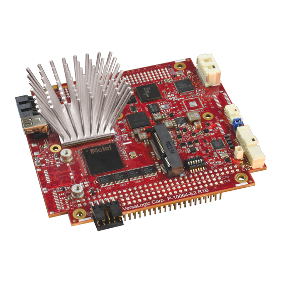
- Page 3 Data sheets and manufacturers’ links for chips used in this product BIOS information and upgrades Utility routines and benchmark software The VersaTech KnowledgeBase is an invaluable resource for resolving technical issues with your VersaLogic product. VersaTech KnowledgeBase EPM-39 Programmer’s Reference Manual...
-
Page 4: Table Of Contents
Contents Introduction ........................1 Related Documents ......................1 System Resources and Maps ..................2 Memory Map ........................2 Interrupts ..........................2 FPGA Registers ......................4 FPGA I/O Space ......................... 4 ISA Bus Addressing and LPC I/O and Memory Map ........... 4 FPGA Register Map ...................... - Page 5 Contents Table 17: AUXOUT – AUX GPIO Output Control Register ........... 16 Table 18: AUXIN – AUX GPIO Input Status Register ............ 17 Table 19: AUXICR – AUX GPIO Interrupt Mask Register ..........17 Table 20: AUXISTAT – AUX GPIO Interrupt Status Register ........17 Table 21: AUXMODE1 –...
-
Page 6: Introduction
Introduction This document provides information for users requiring register-level information for developing applications with the VL-EPM-39. Related Documents The following documents available are on the EPM-39 Product Support Web Page: EPM-39 Hardware Reference Manual – provides information on the board’s hardware features including connectors and all interfaces. -
Page 7: System Resources And Maps
System Resources and Maps Memory Map Table 1: Memory Map Address Range Description 00000h – 9FFFFh Legacy system (DOS) area A0000h – B7FFFh ISA memory area (VGA frame buffer is not accessible) B8000h – BFFFFh Text mode buffer C0000h – CFFFFh Video BIOS area D0000h –... -
Page 8: Table 2: I/O Map
System Resources and Maps Table 2: I/O Map I/O Address Range Device/Owner 3F8h – 3FFh COM1 serial port default 400h – 47Fh ACPI / Power management (reserved) 500h – 5FFh PCH GPIO (reserved) C80h – CBBh EPM-39 FPGA Board Control Registers CBCh –... -
Page 9: Fpga Registers
FPGA Registers FPGA I/O Space The FPGA is mapped into I/O space on the LPC bus FPGA access: LPC I/O space FPGA access size: All 8-bit byte accesses (16-bit like registers are aligned on 16-bit word boundaries to make word access possible in software but the LPC bus still splits the accesses into two 8-bit accesses) ... -
Page 10: Fpga Register Map
FPGA Register Map Register Access Key Reset Status Key Read/Write Power-on reset (only resets one time when input power comes on) Resets prior to the processor entering the S0 power state (that is, at power-on Read-only (status or reserved) Platform and in sleep states) •... - Page 11 FPGA Registers Reset Identifier Offset Address Type RSVD RSVD RSVD RSVD RSVD RSVD RSVD RSVD Reserved RSVD RSVD RSVD RSVD RSVD RSVD FPGA_PSEN MINI_PSDIS MISCSCR1 MISCSR2 USB_HUBMODE W_DISABLE USB_USBID USB_HUBDIS USB_PBDIS USB_OBDIS MISCSR3 Platform RSVD RSVD RSVD RSVD USB_PBOC PBRESET RSVD RSVD Reserved...
- Page 12 FPGA Registers Reset Identifier Offset Address Type UARTMODE2 Platform RSVD RSVD RSVD RSVD RSVD RSVD RSVD FAST_MODE ISACON1 Platform ISA_IRQ11 ISA_IRQ10 ISA_IRQ9 ISA_IRQ7 ISA_IRQ6 ISA_IRQ5 ISA_IRQ4 ISA_IRQ3 ISACON2 Platform RSVD RSVD RSVD RSVD RSVD ISA_IRQ15 ISA_IRQ14 ISA_IRQ12 Reserved RSVD RSVD RSVD RSVD RSVD...
-
Page 13: Fpga Register Descriptions
FPGA Register Descriptions Register Access Key Read/Write Read-only (status or reserved) R/WC Read-status/Write-1-to-Clear RSVD Reserved. Only write 0 to this bit; ignore all read values. RODUCT NFORMATION EGISTERS This register drives the PLED on the paddleboard. It also provides read access to the product code. -
Page 14: Bios And Jumper Status Register
FPGA Registers BIOS UMPER TATUS EGISTER Table 8: SCR –Status/Control Register Identifier Access Default Description RESERVED RESERVED RESERVED Debug LED (controls the yellow LED): LED_DEBUG 0 – LED is off and follows its primary function (MSATA_DAS) 1 – LED is on (indicates FPGA is programmed by default) Status used to indicate that the FPGA is not officially released and is still in a working state. -
Page 15: Timer Registers
FPGA Registers IMER EGISTERS The FPGA implements an 8254-compatible timer/counter that includes three 16-bit timers. Table 9: TICR – 8254 Timer Interrupt Control Register Identifier Access Default Description 8254 Timer interrupt enable/disable: IRQEN 0 – Interrupts disabled 1 – Interrupts enabled 8254 Timer interrupt IRQ select in LPC SERIRQ: 000 –... -
Page 16: Table 10: Tisr - 8254 Timer Interrupt Status Register
FPGA Registers Table 10: TISR – 8254 Timer Interrupt Status Register Identifier Access Default Description RESERVED Reserved. Writes are ignored; reads always return 0. RESERVED Reserved. Writes are ignored; reads always return 0. RESERVED Reserved. Writes are ignored; reads always return 0. RESERVED Reserved. -
Page 17: Table 11: Tcr - 8254 Timer Control Register
FPGA Registers Table 11: TCR – 8254 Timer Control Register Identifier Access Default Description Debug/Test Only: Controls the “gate” signal on 8254 timer #5 when not using an external gate signal: 0 – Gate on signal GCTC5 is disabled TMR5GATE 1 –... -
Page 18: Miscellaneous Fpga Registers
FPGA Registers FPGA R ISCELLANEOUS EGISTERS MISCR1 – Miscellaneous Control Register #1 This is a register in the always-on power well of the FPGA. It holds its state during sleep modes and can only be reset by a power cycle. This is a placeholder register for features like pushing the power-button and also for software initiated resets should those be needed. -
Page 19: Table 13: Miscsr2 - Misc. Control Register #2
FPGA Registers Table 13: MISCSR2 – Misc. Control Register #2 Identifier Access Default Description Determines whether the hub resets only once (to support wake-up from sleep modes on USB ports) or resets every time it enters sleep modes using the platform reset: USB_HUBMODE 0 –... -
Page 20: Table 14: Miscr3 - Misc. Control Register #3
FPGA Registers MISCR3 – Miscellaneous Control Register #3 This register sets the SMBus addresses on the 4-Port PCIe Switch. Table 14: MISCR3 – Misc. Control Register #3 Bits Identifier Access Default Description Reserved 0000 Reserved. Writes are ignored; reads always return 0. Reads the overcurrent status for the USB paddleboard power switches (there are two power switches for the four ports but they have a common overcurrent status). -
Page 21: Table 15: Auxdir - Aux Gpio Direction Control Register
FPGA Registers AUXDIR – AUX GPIO Direction Control Register This register controls the direction of the eight AUX GPIO signals. This reset depends on the state of the FPGA_PSEN signal. If FPGA_PSEN is a ‘0’ then the reset is the power-on and Platform Reset. If FPGA_PSEN is a ‘1’ then this register is only reset at power-on. -
Page 22: Table 18: Auxin – Aux Gpio Input Status Register
FPGA Registers AUXIN – AUX GPIO I/O Input Status Register This registers sets the AUX GPIO input value. It will read the input value regardless of the setting on the direction (that is, it always reads the input). This reads the actual state of the GPIO pin into the part. -
Page 23: Table 21: Auxmode1 – Aux I/O Mode Register
FPGA Registers AUXMODE1– AUX I/O Mode Register #1 These two registers selected the mode on each AUX GPIO. This reset depends on the state of the FPGA_PSEN signal. If FPGA_PSEN is a ‘0’ then the reset is the power-on and Platform Reset. If FPGA_PSEN is a ‘1’... -
Page 24: Table 22: Wdt_Ctl – Watchdog Control Register
FPGA Registers WDT_CTL – Watchdog Control Register Reset type is Platform. Table 22: WDT_CTL – Watchdog Control Register Bits Identifier Access Default Description Watchdog interrupt enable/disable: IRQEN 0 – Interrupts disabled 1 – Interrupts enabled Watchdog interrupt IRQ select in LPC SERIRQ: 000 –... -
Page 25: Table 23: Wdt_Val – Watchdog Value Register
FPGA Registers WDT_VAL – Watchdog Value Register This register sets the number of seconds for a Watchdog prior to enabling the watchdog. By writing this value, the watchdog can be prevented from “firing”. A watchdog fires whenever this registers value is all 0s, so it must be set to a non-zero value before enabling the watchdog to prevent an immediate “firing”. -
Page 26: Table 25: Auxmode2 - Aux I/O Mode Register #2
FPGA Registers AUXMODE2– AUX I/O Mode Register #2 This register defines the interrupt mapping for the AUX GPIOs. Reset type is Platform. Table 25: AUXMODE2 - AUX I/O Mode Register #2 Bits Identifier Access Default Description AUX GPIO interrupt enable/disable: IRQEN 0 –... - Page 27 FPGA Registers TEMPICR – Temperature Interrupt Control Register This is the interrupt mask register for the temperature sensor thermal alerts and the DDR3 SODIMM EVENT signals and the interrupt enable and selection. The SODIMM may not have any temperature event capability. Reset type is Platform. Table 26: TEMPICR –...
- Page 28 FPGA Registers UART1CR – UART1 Control Register (COM1) Reset type is Platform. Note: The BIOS (via ACPI) may modify this register when in an ACPI-capable operating system. The register can be read for status purposes but do not write to it unless you are using a non-ACPI operating system.
- Page 29 FPGA Registers UARTMODE1 – UART MODE REGISTER #1 When the COM Transceiver Mode is set to RS422/485 (in the XCVRMODE register) and the RS-485 Automatic Direction Control is enabled (e.g., UART1_485ADC set to ‘1’) then the transceiver Tx output is enabled when there are bytes to transmit and the transceiver Tx output is disabled (i.e., tri-stated) when there are no bytes to transmit.
- Page 30 FPGA Registers Note: ISA bus if the FPGA UARTs are not used). This means that the UART must be enabled before accessing registers. EPM-39 Programmer’s Reference Manual...
- Page 31 FPGA Registers UARTMODE2 – UART MODE REGISTER #2 Standard software (the BIOS and the operating system) assumes the baud-rate clock is 1.8432 MHz and programs the divisors accordingly; however, a faster oscillator is needed for baud rates higher than 115,200. The FAST_MODE bit in this register is used to shift the divisor by 4 bits (multiply by 16) so that the legacy baud rate comes out correctly for the 16x UART clock.
- Page 32 FPGA Registers ISACONx (x = 1,2) – ISA Control Registers These register are used to enable ISA interrupts on the LPC SERIRQ. ISA interrupts simply pass through to SERIRQ and - per the ISA bus standard - are always high-true. The SERIRQEN control bit is not used for the ISA interrupt mask and should not be set until the interrupt processing is ready.
-
Page 33: Programming Information For Hardware Interfaces
Programming Information for Hardware Interfaces Processor WAKE# Capabilities The following devices can wake up the processor using the PCIE_WAKE# signal to the SoC: Ethernet port 0 controller FPGA via the AUX connector GPIO(3) secondary function The following USB devices can wake up the processor using the in-band SUSPEND protocol: ...
Need help?
Do you have a question about the SandCat and is the answer not in the manual?
Questions and answers