Table of Contents
Advertisement
Quick Links
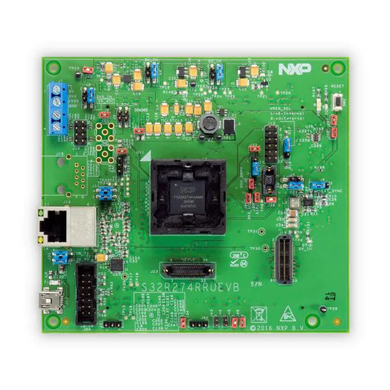
S32R274 EVB
User Guide
Revision 1.4 (SCH-28921_D)
by: Ewan Harwood
Applications Engineering
NXP EKB, UK
1
Introduction
This user's manual details the setup and configuration of
the NXP S32R274 Evaluation Board (hereafter referred to
as the EVB). The EVB is intended to provide a
mechanism for easy customer evaluation of the S32Rxx
family of microprocessors, and to facilitate hardware and
software development.
At the time of writing this document, the S32Rxx family
form the basis of the RADAR specific 55nm devices. For
the latest product information, please speak to your NXP
representative or consult the S32Rxx website at
www.nxp.com.
The EVB is intended for bench / laboratory use and has
been designed using normal temperature specified
components (+70°C).
Contents
S32R274 EVB User Guide ............................................... 2
1
Introduction ............................................................ 2
1.1 List of Acronyms ................................................ 3
1.2 Modular Concept ............................................... 3
1.3 Daughter Card Availability ................................. 4
2
EVB Features ......................................................... 4
3
Configuration .......................................................... 5
3.1 Power Supply Configuration .............................. 6
3.1.1 Motherboard Power Supply Connectors ............ 7
3.1.2 Regulator Power Jumpers ................................. 7
3.1.3 Power Switch, Status LEDs and Fuse ............... 8
3.2 CAN Configuration............................................. 8
3.3 RS232 Configuration ....................................... 10
3.4 LIN Configuration ............................................ 11
3.5 FlexRAY Configuration .................................... 12
3.6 Ethernet Configuration ..................................... 13
3.7 Motherboard .................................................... 13
Configuration - Daughter card.............................. 16
4
4.1 MCU Power ..................................................... 17
4.1.1 Supply Routing and Jumpers ........................... 17
4.1.2 Daughter Card Standalone Power Input .......... 18
4.2 Reset Circuit .................................................... 18
4.3 MCU External Clock Circuit ............................. 19
4.4 JTAG ............................................................... 20
4.5 Nexus Aurora .................................................. 21
4.6 Serial Interprocessor Interface (SIPI) ............... 21
4.7 Camera Serial Interface (MIPI-CSI2) ............... 22
4.8 Gigabit Ethernet .............................................. 22
4.9 CAN FD ........................................................... 23
4.10 Test Points - Daughter Card ............................ 24
25
4.12 Configuring External VREG Mode ................... 26
4.13 Configuring Internal VREG Mode .................... 27
5 Board Interface Connector .......................................... 28
6
Default Jumper Summary Table ........................... 36
6.1 Default Jumper Table - Motherboard ............... 36
6.2 User Area ........................................................ 38
6.3 Known Issues .................................................. 38
Advertisement
Table of Contents

Related Manuals for NXP Semiconductors S32R274 EVB


Summary of Contents for NXP Semiconductors S32R274 EVB
-
Page 1: Table Of Contents
S32R274 EVB Contents S32R274 EVB User Guide ..........2 User Guide Introduction ............2 1.1 List of Acronyms ..........3 1.2 Modular Concept ..........3 1.3 Daughter Card Availability ......... 4 EVB Features ............4 Revision 1.4 (SCH-28921_D) Configuration ............5 3.1 Power Supply Configuration ...... -
Page 2: List Of Acronyms
S32R274 EVB User Guide List of Acronyms Table 1 provides a list and description of acronyms used throughout this document. Table 1. List of Acronyms Acronym Description 1.25V_SR Supply voltage from the 1.25V switching regulator 3.3V_SR Supply voltage from the 3.3V switching regulator 5V_LR Supply voltage from the 5.0V linear regulator... -
Page 3: Daughter Card Availability
S32R274 EVB User Guide Figure 1. Figure 1. Modular concept – Mother board and MCU daughter card Please consult the website at www.nxp.com or speak to your NXP representative for more details on the availability of MCU daughter cards. NOTE For details on your specific daughter card, please consult the instructions included with the daughter card. -
Page 4: Configuration
S32R274 EVB User Guide • All MCU signals readily accessible at a port-ordered group of 0.1” pitch headers • RS232/SCI physical interface and standard DB9 female connector • FlexRAY interface • LINFlexD interface • 2 CAN interfaces, one configurable to be connected to one out of two CAN modules, and one connected to a dedicated third CAN module •... -
Page 5: Power Supply Configuration
S32R274 EVB User Guide Figure 2. Figure 2. EVB Functional Blocks Power Supply Configuration The EVB requires an external power supply voltage of 12V DC, minimum 1.5A. This allows the EVB to be easily used in a vehicle if required. The single input voltage is regulated on-board using three switching regulators to provide the necessary EVB and MCU operating voltages of 5.0V, 3.3V and... -
Page 6: Motherboard Power Supply Connectors
S32R274 EVB User Guide 3.1.1 Motherboard Power Supply Connectors 2.1mm Barrel Connector – P26: Figure 3. Figure 3. 2.1mm Power Connector Screw Terminal Power Connector – P33: This can be used to connect a bare wire lead to the EVB, typically from a laboratory power supply. The polarisation of the connectors is clearly marked on the EVB (Pin 1 = +12v). -
Page 7: Power Switch, Status Leds And Fuse
S32R274 EVB User Guide All of the regulators have the option of being disabled/enabled if they are not required. By default (jumpers are off), all of the switching regulators are enabled and the 5V linear regulator is disabled. The regulators can be enabled individually by the following jumper settings: •... - Page 8 S32R274 EVB User Guide Figure 5. Figure 5. CAN DB9 connector pinout For flexibility, the CAN transceiver I/Os are also connected to two standard 0.1” connectors (P4 and P5) at the top side of the PCB. The pin-out for these connectors is shown in Figure 6.
-
Page 9: Rs232 Configuration
S32R274 EVB User Guide Jumper Label Description 1-2: 5.0V_SR to PHY U1 V 3-4: 12V to PHY U1 V PHY U1 TX to MCU 1-2: TTCAN TX 2-3: MCAN1 TX PHY U1 RX to MCU 1-2: TTCAN RX 2-3: MCAN1 RX... -
Page 10: Lin Configuration
S32R274 EVB User Guide LIN Configuration The EVB is fitted with an NXP MC33661F LIN transceiver (U50) and two different style connectors: A standard LIN Molex connector (J14) at the edge of the board and a standard 0.1" connector (P3). -
Page 11: Flexray Configuration
S32R274 EVB User Guide FlexRAY Configuration The EVB is fitted with two FlexRAY transceivers, a female DB9 connector (for both transceivers) and two alternative connectors. Jumpers J27 and J30 are provided to route the respective MCU signals to the physical interfaces. -
Page 12: Ethernet Configuration
S32R274 EVB User Guide Jumper Label Description FR_A 1-2: PHY U4 TX to MCU 3-4: PHY U4 TXEN to MCU 5-6: PHY U4 RX to MCU FR_A PHY U4 configuration: 1-2: 3.3V (V ) to BGE 3-4: 3.3V (V ) to EN 5-6: 3.3V (V... - Page 13 S32R274 EVB User Guide Signal TP name Shape Description GT11 Hook Ground reference 1.25V_SR User Area Pin 1.25V_SR reference 1.25V_SR 1.25V_SR reference User Area Pin 1.25V_SR User Area Pin 1.25V_SR reference 1.25V_SR User Area Pin 1.25V_SR reference 3.3V_SR User Area Pin 3.3V_SR reference...
- Page 14 S32R274 EVB User Guide Signal TP name Shape Description FR_DBG1 TP11 FlexRAY debug1 FR_DBG2 TP12 FlexRAY debug2 FlexRAY debug3 FR_DBG3 TP13 FEC 25MHz Ethernet clock...
-
Page 15: Configuration - Daughter Card
S32R274 EVB User Guide Configuration – Daughter card This section details the configuration of each of the daughter card’s functional blocks. The daughter card has been designed with ease of use in mind and has been segmented into functional blocks as shown in Figure 12. Detailed silkscreen legend has been used throughout the board to identify all switches, jumpers and user connectors. -
Page 16: Mcu Power
S32R274 EVB User Guide MCU Power 4.1.1 Supply Routing and Jumpers The different MCU supply inputs are connected to the regulators on the motherboard through the interface connector. Figure 13 shows how the MCU power domains are connected to the regulators. -
Page 17: Daughter Card Standalone Power Input
S32R274 EVB User Guide Table 8. MCU power selection jumpers Jumper Description Connects Digital HV supplies to 3.3V_SR Connects Digital LV supplies to 1.25V_SR Connects AFE Supply to 3.3V_LR via LDO Connects AFE Supply to 3.3V_SR via LDO 4.1.2 Daughter Card Standalone Power Input A terminal power input is provided on the daughter card to enable use of the daughter card without the motherboard. -
Page 18: Mcu External Clock Circuit
S32R274 EVB User Guide The reset switch SW2 can be used to reset the MCU. The reset switch signal is connect to the MCU reset signals RESET_B (through jumper J47) and the connection can be released by lifting the according jumper. -
Page 19: Jtag
S32R274 EVB User Guide The clock circuitry for the daughter card is shown in Figure 16. Each source is selectable via the 0-ohm links as shown, with crystal Y3 being the default factory option. Figure 16. 40MHz crystal circuit JTAG The EVB is fitted with 14-pin JTAG debug connector. -
Page 20: Nexus Aurora
S32R274 EVB User Guide Nexus Aurora Table 10 shows the pinout of the 34-pin Samtec connector for the S32R274. Table 10. Aurora Trace connector pinout Pin No Function Pin No Function TX0+ VREF TX0- TCK/TCKC/DRCLK TMS/TMSC/TxDataP TX1+ TDI/TxDataN TX1- TDO/RxDataP... -
Page 21: Camera Serial Interface (Mipi-Csi2)
S32R274 EVB User Guide Camera Serial Interface (MIPI-CSI2) A dedicated MIPI-CSI2 interface is provided on the daughtercard, and is designed to provide compatibility with the Eagle MR3003 Radar front end EVK. To preserve signal integrity MIPI-CSI2 signals are not routed to the motherboard. -
Page 22: Can Fd
S32R274 EVB User Guide Figure 20. RGMII Signal Connections to Motherboard CAN FD Although the EVB motherboard supports CAN, 2x NXP TJA1051T/3 CAN FD (Flexible Data) compliant physical interfaces are provided (U14 and U16) on the daughtercard for higher speed applications. -
Page 23: Test Points - Daughter Card
S32R274 EVB User Guide Similarly CAN2 signals can be routed to either the on-board CAN-FD phy U16 via J43 and J44, or to the motherboard Flexray physical interface via J46 and J45. Figure 21. CAN FD Physical Interfaces 4.10 Test Points - Daughter Card Daughter card test points are listed and detailed in Table 11. -
Page 24: Configuring The Daughter Card For Standalone Use
S32R274 EVB User Guide Power good signal from 3V3_PGOOD Surface Pad 3.3v linear regulator Power good signal from 4V2_PGOOD Surface Pad 4.2v switching regulator 4.2V Switching regulator 4V2_SW_REG Surface Pad output 1.2V Ethernet phy 1V2_LR_HV Surface Pad regulator output 1.25V_SR_LDO Surface Pad 1.25V Core supply... -
Page 25: Configuring External Vreg Mode
S32R274 EVB User Guide 4.12 Configuring External VREG Mode Table 12 shows the jumper configuration for the EVB when in external VREG mode. Table 12. Jumper Configuration for External VREG mode Jumper Number Default position Function 1.25v supply 5.0v supply to create 3.3v for the AFE Regulator 3.3v supply for the device... -
Page 26: Configuring Internal Vreg Mode
S32R274 EVB User Guide 4.13 Configuring Internal VREG Mode Table 13 shows the jumper configuration for the EVB when in internal VREG mode. Table 13. Jumper Configuration for Internal VREG mode Jumper Number Default position Function 1.25v supply 5.0v supply to create 3.3v for the AFE Regulator 3.3v supply for the device... -
Page 27: Board Interface Connector
S32R274 EVB User Guide 5 Board Interface Connector This chapter provides a useful cross reference to see the connection from the motherboard to the board interface connector, and what MCU pins are connected to the interface connector on the daughter card. - Page 28 S32R274 EVB User Guide 257 BGA (SCH 257 BGA (SCH Connector Motherboard Connector Motherboard NAME) NAME) Link Link A-11 B-230 GPIO 22 (CLKOUT0) A-12 B-229 ADC0_AN0 A-13 B-228 ADC0_AN1 A-14 B-227 GPIO 9 (PA9) ADC0_AN11 A-15 PA10 B-226 PB10 GPIO 10 (DSPI2_CS0)
- Page 29 S32R274 EVB User Guide 257 BGA (SCH 257 BGA (SCH Connector Motherboard Connector Motherboard NAME) NAME) Link Link A-45 B-196 A-46 B-195 A-47 B-194 ADC0_AN_5 A-48 B-193 A-49 B-192 ADC0_AN_7 A-50 B-191 ADC0_AN_8 A-51 B-190 ADC0_AN_4 A-52 B-189 ADC0_AN_6 A-53...
- Page 30 S32R274 EVB User Guide 257 BGA (SCH 257 BGA (SCH Connector Motherboard Connector Motherboard NAME) NAME) Link Link A-78 PG13 B-163 PH13 GPIO 125 (PH13) A-79 PG14 B-162 PH14 A-80 PG15 B-161 PH15 A-81 5.0V_SR B-160 3.3V_SR 5.0V_SR 3.3V_SR A-82 5.0V_SR...
- Page 31 S32R274 EVB User Guide 257 BGA (SCH 257 BGA (SCH Connector Motherboard Connector Motherboard NAME) NAME) Link Link A-114 B-127 A-115 PK10 B-126 PL10 A-116 PK11 B-125 PL11 A-117 PK12 B-124 PL12 A-118 PK13 B-123 PL13 A-119 PK14 B-122 PL14...
- Page 32 S32R274 EVB User Guide 257 BGA (SCH 257 BGA (SCH Connector Motherboard Connector Motherboard NAME) NAME) Link Link A-150 B-91 A-151 B-90 A-152 B-89 A-153 B-88 A-154 B-87 A-155 PO10 B-86 PP10 A-156 PO11 B-85 PP11 A-157 PO12 B-84 PP12...
- Page 33 S32R274 EVB User Guide 257 BGA (SCH 257 BGA (SCH Connector Motherboard Connector Motherboard NAME) NAME) Link Link A-186 B-55 A-187 B-54 A-188 B-53 A-189 B-52 A-190 B-51 A-191 B-50 A-192 B-49 A-193 B-48 A-194 B-47 A-195 PS10 B-46 PT10...
- Page 34 S32R274 EVB User Guide 257 BGA (SCH 257 BGA (SCH Connector Motherboard Connector Motherboard NAME) NAME) Link Link A-222 B-19 3.3v_SR_LDO 3.3v_SR_LDO VDD_HV_IO_MAIN VDD_HV_IO_MAIN A-223 B-18 3.3v_SR_LDO 3.3v_SR_LDO VDD_HV_IO_MAIN VDD_HV_IO_MAIN A-224 B-17 3.3v_SR_LDO 3.3v_SR_LDO VDD_HV_IO_MAIN VDD_HV_IO_MAIN A-225 B-16 A-226 B-15...
-
Page 35: Default Jumper Summary Table
S32R274 EVB User Guide 6 Default Jumper Summary Table The details for the DEFAULT jumper configuration of the EVB as set up on delivery can be found in Table 12 and Table 13 depending on the required regulation mode. 6.1 Default Jumper Table - Motherboard On delivery the motherboard comes with a default jumper configuration. - Page 36 S32R274 EVB User Guide Jumper Default Pos PCB Legend Description FR-A PHY U4 configuration: 1-2: 3.3V (V ) to BGE 3-4: 3.3V (V ) to EN 5-6: 3.3V (V ) to STBY 7-8: GND to WAKE FR_PWR FlexRAY transceiver VIO selection...
-
Page 37: User Area
S32R274 EVB User Guide Jumper Default Pos PCB Legend Description ADC_VSUP Connect EVB supply voltages to analog inputs 12V (4.3V) Connect 12V (scaled to 4.3V) EVB power to analog input ENABLE Enable 5V linear regulator DISABLE Disable 1.25V switching regulator DISABLE Disable 3.3V switching regulator... - Page 38 S32R274 EVB User Guide How to Reach Us: Home Page: www.nxp.com E-mail: support@nxp.com USA/Europe or Locations Not Listed: NXP Semiconductor Technical Information Center, CH370 1300 N. Alma School Road Chandler, Arizona 85224 +1-800-521-6274 or +1-480-768-2130 support@nxp.com Europe, Middle East, and Africa:...
- Page 39 Mouser Electronics Authorized Distributor Click to View Pricing, Inventory, Delivery & Lifecycle Information: S32R274RRUEVB...
Need help?
Do you have a question about the S32R274 EVB and is the answer not in the manual?
Questions and answers