
Related Manuals for NXP Semiconductors S32K3X4EVB-Q257


Summary of Contents for NXP Semiconductors S32K3X4EVB-Q257
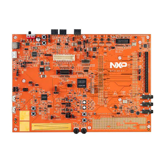
- Page 1 S32K3X4EVB-Q257 S32K3X4EVBQ257ND Customer Evaluation Board for S32K3x4 MCUs Hardware User Manual...
-
Page 2: Table Of Contents
Power supply ................................ 9 S32K3X4EVB-Q257 - Main Power Supply ....................... 9 S32K3X4EVB-Q257 – FS26/Modes Operation ....................10 S32K3X4EVB-Q257 – +5.0 Volts Power Supply .................... 11 S32K3X4EVB-Q257 – +3.3 Volts Power Supply .................... 12 S32K3X4EVB-Q257 – VDD_HV_A ........................ 12 Programming and Debug Interface ........................17 RESET Switch and LED indicator ........................ -
Page 3: Definitions, Acronyms, And Abbreviations
S32K3X4EVB-Q257 | S32K3X4EVBQ257ND HWUM NXP Semiconductors Hardware User Manual 2 Definitions, Acronyms, and Abbreviations The following list defines the abbreviations used in this document. Compact Disk CMOS Complementary Metal Oxide Semiconductor CPLD Custom Programmed Logic Devices Central Processing Unit Camera Sensor Imaging... -
Page 4: Block Diagram
S32K3X4EVB-Q257 | S32K3X4EVBQ257ND HWUM NXP Semiconductors Hardware User Manual 3 Block Diagram Figure 1. S32K3X4EVB-Q257 | S32K3X4EVBQ257ND – Block diagram 4 Features IMPORTANT • Verify and download the last version of this document in http://www.nxp.com • Before the S32K344 Customer Evaluation board is used or power is applied, please fully read this user manual. -
Page 5: Default Configuration
S32K3X4EVB-Q257 | S32K3X4EVBQ257ND HWUM NXP Semiconductors Hardware User Manual Figure 2. S32K3X4EVB-Q257 – Features 5 Default Configuration Table 1. S32K3X4EVB-Q257 - Default Configuration S32K3X4 S32K3X4 EVB- Interface EVBQ257 Reference / Signal Configuration Description/Comment Q257 ● ● VDD_HV_A_MCU +5.0V The VDDA_HV_A domain is connected Power to +5.0V–... - Page 6 S32K3X4EVB-Q257 | S32K3X4EVBQ257ND HWUM NXP Semiconductors Hardware User Manual S32K3X4 S32K3X4 Interface EVB- EVBQ257 Reference / Signal Configuration Description/Comment Q257 ● ● QSPI-A Enabled The MCU signals to the QSPI-A Memory Memory Interface are enabled ● Open SDA PTA15 PTA15/LPUART6_RX...
-
Page 7: S32K3X4Evb-Q257 And S32K3X4Evbq257Nd - Startup
Follow these steps to connect and power on the board Carefully unpack the S32K3X4EVB-Q257 and observe ESD preventive measures while handling the K3 development board. Connect necessary cables between host PC and EVB board prior to applying power to the EVB. - Page 8 Indicates that the +3.3Vlinear regulator is enabled and working correctly. Figure 3. S32K3X4EVB-Q257 | S32K3X4EVBQ257ND – Power supply Input and LED power indicators If no LED’s are illuminated when power is applied to the EVB and the regulators are correctly enabled using the appropriate jumpers, it is possible that either power supply is not connected properly, or the voltage level is lower that the specified [+12.0V...
-
Page 9: Power Supply
+5.0V, +3.3V and +1.5V, for the different power configurations of VDD_HV_A, VDD_HV_B, V15 and other interfaces. 7.1 S32K3X4EVB-Q257 - Main Power Supply Figure 4. S32K3X4EVB-Q257 | S32K3X4EVBQ257ND – Main power supply input Table 2. Main power supply connectors Connector Description 2.1mm Barrel Connector –... -
Page 10: S32K3X4Evb-Q257 - Fs26/Modes Operation
R1968 C3851 R1971 R1963 C3847 R1969 10uF MMSZ8V2T1G 0.1uF 0402 Figure 5. S32K3X4EVB-Q257 | S32K3X4EVBQ257ND – FS26/Modes Operation Table 3. S32K3X4EVB-Q257 – FS26/Modes Operation Reference Jumper Position Description Comments Flash Mode J686 The R1961 resistor to VBATP (VBAT [Default protected +12.0V) is routed as pull-up to the configuration] VDEBUG Pin. -
Page 11: S32K3X4Evb-Q257 - +5.0 Volts Power Supply
FS26_VLDO1 SILK = P5V0 P5V0 5V0 OUTPUT SILK = P5V0 JUMPER(Default) = 1-2 Closed Figure 6. S32K3X4EVB-Q257 | S32K3X4EVBQ257ND – General jumper for the P5V0 (+5.0V) reference Table 4. S32K3X4EVB-Q257 – +5.0 Volts Power Supply Reference Jumper Position Description Comments The +5.0V output of the FS26x SBC [FS26_VLDO1] is routed... -
Page 12: S32K3X4Evb-Q257 - +3.3 Volts Power Supply
S32K3X4EVB-Q257 | S32K3X4EVBQ257ND HWUM NXP Semiconductors Hardware User Manual 7.4 S32K3X4EVB-Q257 – +3.3 Volts Power Supply Figure 7. S32K3X4EVB-Q257 | S32K3X4EVBQ257ND – General jumper for the P3V3 (+3.3V) reference Table 5. S32K3X4EVB-Q257 – +.3.3 Volts Power Supply Reference Jumper Position... - Page 13 S32K3X4EVB-Q257 | S32K3X4EVBQ257ND HWUM NXP Semiconductors Hardware User Manual Table 6. S32K3X4EVB-Q257 – VDD_HV_A Reference Jumper Position Description Comments P5V0 (+5.0V Switching Power Supply) is selected for the Default VDD_HV_A_MCU reference closed P3V3_DC_SW (+3.3V Switching Power Supply) is selected for the VDD_HV_A_MCU reference...
- Page 14 1-2 -- CLOSED HDR 1X2 [Default Position] Voltage Domain 0.1uF 0402 Figure 9. S32K3X4EVB-Q257 | S32K3X4EVBQ257ND – Main power supply Table 7. S32K3X4EVB-Q257 – VDD_HV_B Reference Jumper Position Description Comments P5V0 (+5.0V Switching Power Supply) is selected for the VDD_HV_B_MCU reference P3V3_DC_SW (+3.3V Switching Power Supply) is...
- Page 15 VDD_HV_A_MCU FS26_VREF VDD_REFH TP264 J410 SILK = VREFH_MCU HDR 1X3 JUMPER(Default) = 1-2 Closed Figure 10. S32K3X4EVB-Q257 | S32K3X4EVBQ257ND – VREFH power supply Table 8. S32K3X4EVB-Q257 – VREFH Reference Jumper Position Description Comments J410 The VREFH_MCU reference is routed to Default closed the VDD_HV_A_MCU domain.
- Page 16 V15_MCU S32K3XX External Supply for V11 Internal Core Logic Voltage Supply Figure 11. S32K3X4EVB-Q257 – V15 power supply Table 9. S32K3X4EVB-Q257 – V15 Domain Reference Jumper Position Description Comments The VDD_HV_A domain is routed to the collector terminal in order to supply the NPN external Ballast transistor for the V15_MCU domain.
-
Page 17: Programming And Debug Interface
Figure 12. S32K3X4EVB-Q257 | S32K3X4EVBQ257ND – RESET Switch 8.2 On-board S32K3 Debugger The S32K3X4EVB-Q257 [only] incorporates an On-Board Debugger embedded well as JTAG connectors. It bridges serial and debug communications between a USB host and an embedded target processor. S32K3X4EVB-Q257 HWUM All Information provided in this document is subject to legal disclaimers ©... - Page 18 S32K3X4EVB-Q257 | S32K3X4EVBQ257ND HWUM NXP Semiconductors Hardware User Manual Figure 13. S32K3X4EVB-Q257 | S32K3X4EVBQ257ND – On-board S32K3 Debugger Table 10. Programming and Debug Connectors S32K3X4EVB-Q257 Connector Description S32K3X4EVBQ257ND 20-Pin Cortex This small 20-pin (0.05") connector provides access to Debug + ETM...
-
Page 19: Usb To Serial Interface
Note that only one of these is used so you will need to try both. For more information on the USB drivers and general fault finding, consult the FTDI website at http://www.ftdichip.com/ Figure 14. S32K3X4EVB-Q257 | S32K3X4EVBQ257ND – USB to Serial Interface The PTC27 MCU port ( ) and PTC26 MCU port (... - Page 20 S32K3X4EVB-Q257 | S32K3X4EVBQ257ND HWUM NXP Semiconductors Hardware User Manual Table 11. USB to serial interface - Control Jumpers Signal Reference Description Comment /Module Port LPUART13_RX PTC26 R303 LPUART13_RX signal is routed to FTDI Default configuración interface LPUART13_TX PTC27 R309 LPUART13_TX signal is routed to FTDI Default configuración...
-
Page 21: Lin Interface
TJA1021T/20/C, supporting both master and slave mode (jumper selectable). The output from the LIN transceivers is connected to J675. Figure 15. S32K3X4EVB-Q257 | S32K3X4EVBQ257ND – V15 power supply The pinout of these headers is shown below and is also detailed on the PCB silkscreen. - Page 22 R1881 10.0K TJA1021T/20/C C3839 R1155 R1885 100pF 0402 0402 0402 10.0K 10.0K Figure 16. S32K3X4EVB-Q257 | S32K3X4EVBQ257ND – LIN Physical Layer1 TJA1021HG: Quad LIN 2.2A/SAE J2602 transceiver J678 VDD_HV_A_PERH VDD_HV_B_PERH HDR 1X2 0402 TP270 R1896 0402 T PAD VBATP_SW R1897...
-
Page 23: Can Interface
S32K3X4EVB-Q257 | S32K3X4EVBQ257ND HWUM NXP Semiconductors Hardware User Manual 11 CAN Interface Figure 18. S32K3X4EVB-Q257 | S32K3X4EVBQ257ND – CAN Interface Table 14. CAN Interface - Connectors Circuit/ Connector Reference Signal/Connection Interface Number CAN0 CANH0 CANL0 J673 CAN1 CANH1 CANL1 S32K3X4EVB-Q257 HWUM All Information provided in this document is subject to legal disclaimers ©... - Page 24 R1205 R1331 R1333 TJA1153 0.1uF 0402 0402 0402 0402 0402 Figure 19. S32K3X4EVB-Q257 | S32K3X4EVBQ257ND – CAN Physical Layer0 - TJA1153 Secure HS-CAN Transceiver TP266 TP267 T PAD T PAD CAN Output to ARDUINO Connectors P5V0 VDD_HV_B_PERH ------------------------------------------ BLM18KG121T Z1...
-
Page 25: Ethernet Interface
+3.3V and +12.0V (+5.0V as optional) to the ethernet connector. Figure 21. S32K3X4EVB-Q257 | S32K3X4EVBQ257ND – CAN Physical Layer1 - TJA1153 Secure HS-CAN Transceiver Ethernet Connector - The EVB has a High-Speed Connector that is compatible with some external boards: •... -
Page 26: Ethernet Mii/Rmii Connector - Pinout
0603 0.22UF 0402 50MHZ P3V3_ENET HDR 1X1 R480 Page[11] ENET_MII_TX_ER R481 Figure 23. S32K3X4EVB-Q257 | S32K3X4EVBQ257ND – Ethernet MII/RMII Connector Table 16. Ethernet MII/RMII Configuration MODULE SIGNAL DESCRIPTION /COMMENT /FUNCTION PORT MII/RMII ENET_MII_RMII_RXD0 PTD9 All ports routed to the Ethernet MII/RMII signal... - Page 27 S32K3X4EVB-Q257 | S32K3X4EVBQ257ND HWUM NXP Semiconductors Hardware User Manual GPIOs ENET_INH_LS PTA26 ENET_INT_LS PTA27 ENET_RESET PTE5 As optional GPIO for a RESET on the ethernet connector is the PTE21, for this option, R439/0- Ohms must be placed. LPSPIx ENET_SPI_MISO_LS PTC9...
-
Page 28: Qspi-A Configuration
The S32K3 EVB incorporates a MX25L6433F is 64Mb bits Serial NOR Flash memory, which is connected to the QSPIA Module of the S32K344 MCU. Figure 24. S32K3X4EVB-Q257 – CAN Physical Layer1 - TJA1153 Secure HS-CAN Transceiver Table 18. QSPIA Memory Interface - Jumpers... -
Page 29: User Peripherals
Interface) are available at the GPIO matrix as detailed below. The matrix provides an easy to follow, intuitive, space-saving grid of 0.1” header through-hole pads. Users can solder wires, fit headers, or simply insert a scope probe into the respective pad. Figure 26. S32K3X4EVB-Q257 | S32K3X4EVBQ257ND – GPIO Matrix Figure 27. S32K3X4EVB-Q257 | S32K3X4EVBQ257ND – GPIO Matrix... -
Page 30: User Led Indicators
MMBT3904TT1G R666 33K R1179 33K Figure 28. S32K3X4EVB-Q257 | S32K3X4EVBQ257ND – User LED indicators 15.3 User Pushbuttons There are 2 push-buttons active to high (pulled low, driven to VDD_HV_A and VDD_HV_B), the push button switches (SW4 and SW5) connected to MCU ports. The switches are connected as follows:... - Page 31 S32K3X4EVB-Q257 | S32K3X4EVBQ257ND HWUM NXP Semiconductors Hardware User Manual Figure 29. S32K3X4EVB-Q257 | S32K3X4EVBQ257ND – User Pushbuttons VDD_HV_A_PERH TP203 TP204 TPAD TPAD 1825967-2 USERSW _0 R652 10.0K USER_SW0 Page[5] C286 C287 R653 0.1uF 0.1uF 4.7K 0402 0402 VDD_HV_B_PERH TP209 TP210...
-
Page 32: Adc Rotary Potentiometers
There are zero-ohm resistors on the direct connections between each USERSW and the MCU pins. These can be removed if required to isolate or change the User Switch from the default MCU pin. Figure 31. S32K3X4EVB-Q257 | S32K3X4EVBQ257ND – ADC Rotary Potentiometers S32K3X4EVB-Q257 HWUM All Information provided in this document is subject to legal disclaimers ©... -
Page 33: Default Jumpers
Page[5] SILK = ADCPOT1 C1230 C296 0.1uF 0.1uF 0402 0402 Figure 32. S32K3X4EVB-Q257 | S32K3X4EVBQ257ND – ADC Rotary Potentiometers 16 Default Jumpers Table 22. Default Jumper Configuration Reference Position Interface Description / Comments FS26x FS26_VLDO1 [+5.0V] is routed to P5V0 domain FS26_VLDO2 [+3.3V] is routed to P3V3 domain... - Page 34 J672 CAN1 Physical Layer is enabled. VBATP_SW is routed/turning-ON the TJA1153 -U64 Figure 33. S32K3X4EVB-Q257 | S32K3X4EVBQ257ND – Default jumpers’ configuration S32K3X4EVB-Q257 HWUM All Information provided in this document is subject to legal disclaimers © NXP B.V. 2020. All rights reserved REV B –...
-
Page 35: Revision History
S32K3X4EVB-Q257 | S32K3X4EVBQ257ND HWUM NXP Semiconductors Hardware User Manual 17 Revision history Table 23. Revision history Board Schemati Schematic/ Document Name Date c/ Board Board Changes Author Revision Number Revision 08/2021 S32K3X4EVB-Q257 47827 Infernal DRAFT Jesús Sánchez 09/2021 S32K3X4EVB-Q257 47827... -
Page 36: Legal Information
NXP Semiconductors products in order to included in a draft version of a document and shall have no avoid a default of the applications and the products or of the liability for the consequences of use of such information application or use by customer’s third party customer(s).
Need help?
Do you have a question about the S32K3X4EVB-Q257 and is the answer not in the manual?
Questions and answers